 f4hdk
f4hdkThis is a 16 bits RISC CPU, with a very simple instruction decoding.
There is no microcode. Each instruction is very simple, very basic. The complexity usually found in the microcode is transferred to the compiler. The compiler has to generate a complex sequence of simple instructions. The execution code generated is therefore quite huge, but this is not a problem with 2MB of RAM.
The datapath of the CPU-core is mainly “load and store”, and the register C is the central register.
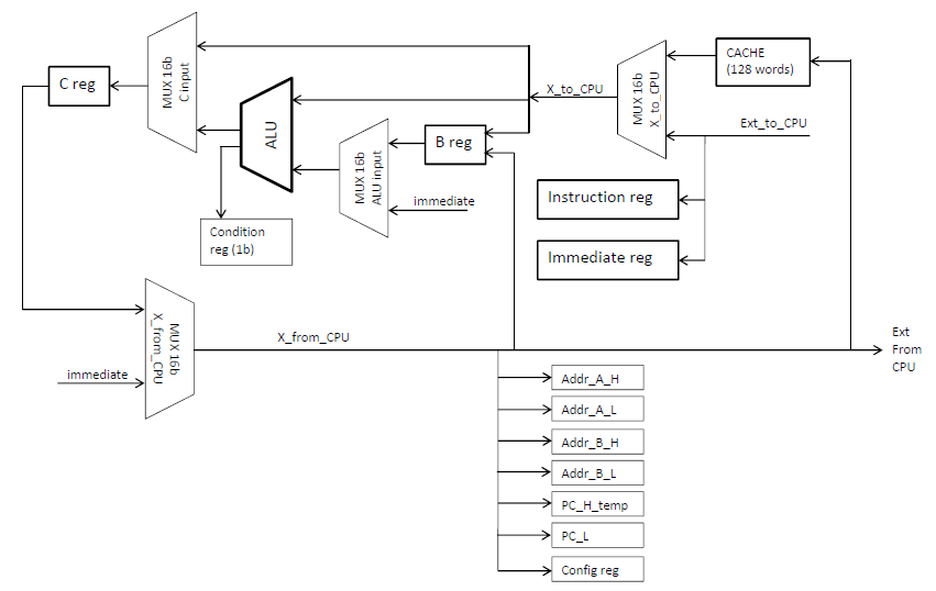
Some instruction can take 16bits of optional “immediate” value, written inside the code.
Therefore, one instruction can take 1 or 2x 16bits of executable code size.
The ALU only computes integers, which is enough for this computer.
CACHE :
1 have put a 128x16bits cache memory inside the FPGA. This cache can be accessed directly with one instruction : the 7-bits address of this cache memory is mapped to the last 16bits of the instruction.
This greatly accelerates access to intermediate data when computing. The compiler uses this cache systematically for intermediate variable of complex formulas.
But this cache memory is accessed at the same speed than external memory. I could have made this with a “zero page”, but at the beginning of the project, I didn’t know this concept.
Optimizations
3 hardware optimisations are available inside the core, which accelerate data copy and sprite manipulations. My first goal was to make 2D graphic games.
These 3 mechanisms are optionally activated via the “config” register of the core.
The compiler is not able to use these options naturally, and the only way to use them is to code in assembly language.
The 3 optimisations are:
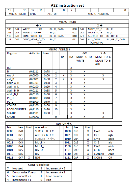
- Hardware loop counter : repetitive loops can be counted in hardware, and the stop condition is computed in hardware, not in software. This is like a “for-next” loop, but faster. The loop counter is decremented at each call of one “goto” instruction. The initial value of “loop counter” (the number of occurrence of loop) shall be written in the “loop counter” register.
- There are 2 separated address registers for data manipulation (A and B), each with a post-increment option. The post-increment can be +1 or +2, to adjust to a word size of 8bits or 16bits. All this help to copy data from one address range to another.
- The last option is “do not copy if zero”, in hardware. This is helpful for transparent sprites. The colour 0x00 means “transparent”
Address computation :
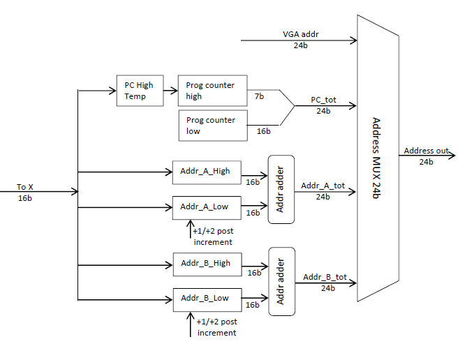
The 24bits address are computed in hardware with a sum of 2 16bits address registers called address low and address high. This helps for manipulating big tables and 2D images. The address high is dedicated to the line address, and address low is dedicated to row address.

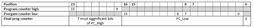
Warning, address manipulated by the program counter manage words in 16bits, omitting the last address bit, unlike data which address are expressed in 8 bits words, whatever their size.
Errors:
The core of the CPU is the first part that I have coded (remember, this is my first FPGA project). I have made quite a lot of errors. This could have made the core compute faster.
The “load and store” architecture is too simple. There is no reason to make such architecture in an FPGA.
I also have integrated a 16bits hardware divider. This is almost useless, and consumes lots of FPGA cells.
When I started this project, I was only little aware of all these aspects, and I learned them while working on it. I discovered these errors too late, while coding the compiler, and I didn’t want to reorganize the project.
Discussions
Become a Hackaday.io Member
Create an account to leave a comment. Already have an account? Log In.