Story
This project is an enhancement to an earlier project previously published:
Microbit Pulse Generator - Variable Ranges
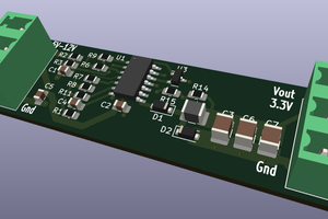
The enhancements are a custom designed PCB to carry out the D2A conversion for the Sine and Sawtooth waveforms complete with independent outputs and independent amplitude control.
With the addition of an OLED display to indicate range, frequency and output status.
All housed in a custom 3D printed enclosure.
Digital waveforms
A digital sinewave waveform can be generated using shift resisters with weighted outputs.
Using two 4 bit shift registers we can generate 8 discrete up steps and 8 discrete down steps for symmetry.
For the first shift register.
With a resistor R on Q0 a current flows when QO is high. If we place a resistor on Q1 that's R./2 then twice the current will flow when Q1 is high. Consequently, if we fit resistors of R/4 on Q2 and R/8 on Q3 then we have a weighted current for each step counting up.
For the second shift register.
With a resistor R on Q3 a current flows when Q3 is high. If we place a resistor on Q2 that's R./2 then twice the current will flow when Q2 is high. Consequently, if we fit resistors of R/4 on Q1 and R/8 on Q0 then we have a weighted current for each step that reduces as the count increases.
If the summing point for both counters is connected to a load resistor each current step generates a corresponding voltage step.
The frequency of the output waveform = Fin/2^(n/2) where n = weighted outputs.
Therefore if Fin = 1KHz then the sinewave frequency will be 1000/16 = ~62.5Hz
Circuit Design
The circuit is designed using low voltage logic IC's (Shift register, Binary Counter, EXOR's and OpAmp) using DIL packages for ease of assembly.
The Sawtooth waveform is generated using a CD4024, 7 bit binary counter with binary weighted resistors connected to the 4 LSB outputs.
The clock input is derived from the MicrobIt at output P0.
The control for the clock frequency is provided by a 100k, 10 turn potentiometer with the main resistance connected between 0V and 3V and the wiper connected to P1 of the Microbit to provide a variable voltage (Vv) that is used to vary the frequency.
Vv = Rx/100k*3V where Rx is the resistance between the wiper and the connection to 0V
A POR (Power On Reset), is provided by a CR* network connected to the reset pins to ensure the Counters and the Registers power up in the low state.
*(The CR network pulls the Reset pin High on power up for ~1mS until the capacitor charges then its maintained low by the resistor).
The Binary Counter increments on each negative transition of the clock advancing one count from 0 to 15 then resets to 0 to repeat the cycle.
The result is a repetitive digital sawtooth wave.
The voltage at the summing point is fed to the non inverting input of one half of a dual Op-Amp configured as a non inverting amplifier.
A 5k (Rf) potentiometer is connected in the feedback path in conjunction with a 220R (Rp) to control the waveform output amplitude. Vgain = 1+Rf/Rp with Vgain from 1 to 24 enabling the output voltage to be controlled from ~0 to 3V.
The Shift Register transfers data on each positive transition of the clock and the last stage (Q3) of register 1 is connected to the data input of register 2 with its last stage (Q3) fed back to the data input of register 1.
At switch on all the registers are reset to zero but the inverter connected to the data input of register 1 sets each stage to a logic 1 on each clock transition. Giving a progressive increase in voltage.
Once the last stage of register 2 is set to 1 the data input is set to 0 by the inverter and each stage is successively set to 0. Giving a progressive reduction in voltage.
The result is a repetitive digital sine wave.
The voltage at the summing point is fed to the non inverting input of one half of a dual Op-Amp configured as a non inverting amplifier.
A 5k (Rf) potentiometer is connected in the feedback path...
Read more »
 Bud Bennett
 Yann Guidon / YGDES
 The Big One