 Tim
TimNow that we managed to define the logic gate implementation and synthesis into a netlist, it is time to figure out how to implement the gates on a PCB. The placementtool PCBPlacer.py in PCBFlow does this by breaking down logic gates into microcells that represent very basic circuit unit. The rationale is to create a minimum set of microcells to simplify the desing. A secondary contrain is that each microcell should be roughly square shaped so that they can be arranged in a grid.
Currently supported gate types:
- NOT
- NAND2
- NAND3
- NAND4
- D-Flipflop
NOT-Gate / Inverter
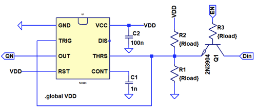
The inverter can be directly implemented by a single NE555, hence it is not broken down further and represented by its on microcell ne_NOT.
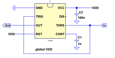
The code to place a NE555 plus decoupling capacitor on the PCB is shown below.
    def insertNE555not(self, x, y, netin, netout, cellname=""):
        """Insert NE555 logic inverter """

        n_elements = self.n_board.find('elements')
        et.SubElement(n_elements, 'element', name = "Q"+cellname, library="discrete_logic_components", package="SOIC-8", value="NE555", x=str(x+1.6), y=str(y+3.7),rot="R90")
        self.countcomponent("NE555")

        self.addcontact('GND'   , "Q"+cellname, "1" ) # GND
        self.addcontact(netin   , "Q"+cellname, "2" ) # TRIG
        self.addcontact(netout  , "Q"+cellname, "3" ) # OUT
        self.addcontact('VCC'   , "Q"+cellname, "4" ) # RESET
#        self.addcontact(''     , "Q"+cellname, "5" ) # CONT
        self.addcontact(netin   , "Q"+cellname, "6" ) # THRESH
#        self.addcontact(''     , "Q"+cellname, "7" ) # DISCH
        self.addcontact('VCC'   , "Q"+cellname, "8" ) # VCC

        # always insert cap
        et.SubElement(n_elements, 'element', name = "C"+cellname, library="discrete_logic_components", package="CAP0402", value="CAP", x=str(x-1.8), y=str(y+3.7),rot="R90")
        self.countcomponent("cap")
        self.addcontact('VCC'  , "C"+cellname, "2" )
        self.addcontact('GND'  , "C"+cellname, "1" )
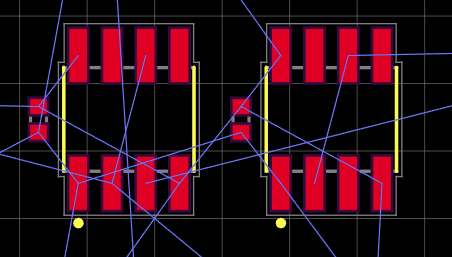
Resulting footprint for two inverters
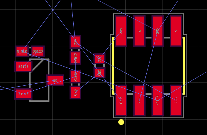
NAND2/NAND3/NAND4
The NAND2 gate can be broken down into a wired AND gate (resistor and diodes) and an inverter, so that each NAND gate is represented by two microcells: ne_NOT, ne_WANDx.
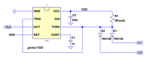
The code will automatically adjust the number of diodes according to the number of inputs
    def insertNE555wand(self, x, y, netins, netout, cellname=""):
        """Insert wired and for NE555 logic """

        n_elements = self.n_board.find('elements')
        et.SubElement(n_elements, 'element', name = "R"+cellname, library="discrete_logic_components", package="RES0402", value="RES", x=str(x+3.25), y=str(y+6.1),rot="R90" )
        self.countcomponent("resistor")
        self.addcontact(netout , "R"+cellname, "1" )
        self.addcontact('VCC'  , "R"+cellname, "2" )

        xofs=0
        num=0
        for curnet in netins:
            et.SubElement(n_elements, 'element', name = "D"+cellname+str(num), library="discrete_logic_components", package="SOD-323", value="1N4148WS", x=str(x+0.75), y=str(y+1+3*1.75-xofs))
            self.countcomponent("diode")
            self.addcontact(netout , "D"+cellname+str(num), "A" )
            self.addcontact(curnet , "D"+cellname+str(num), "C" )
            self.devcounter += 1
            xofs = xofs + 1.75
            num = num + 1
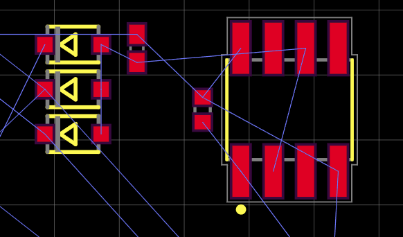
Resulting layout for NAND3
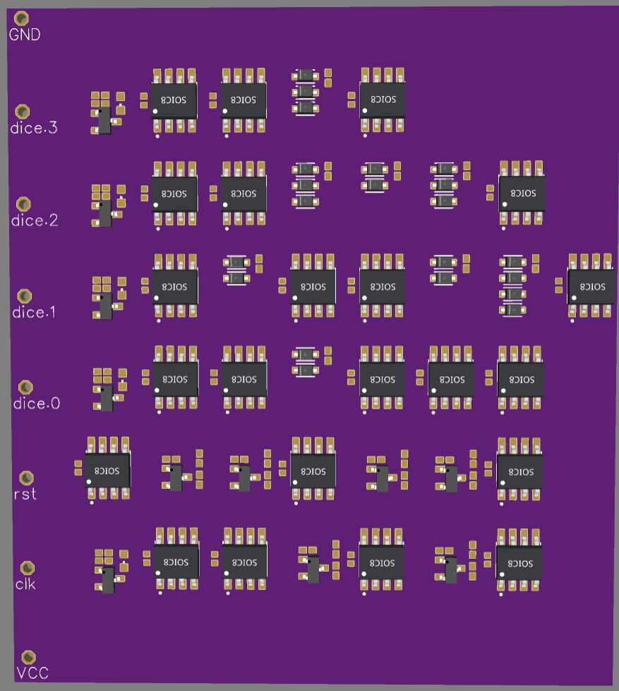
D-Flipflop
The D-Flipflop is implemented as a master and slave latch consisting of an inverter (for the clock) and two latches. Each latch is then broken down into a transmission gate (transistor+3x resistor) ne_TBUF and an inverter. ne_NOT.
In total, each DFF is broken down into five microcells (3x ne_NOT, 2x ne_TBUF). I implemented some code to remove redundant clock inverters, so that some DFF can be reduced to four microcells. This is possible due to the push/pull output of the NE555.
The layout for one latch, consisting of ne_BUF and ne_NOT is shown below.
Having completed all the microcells, we can now generate a full PCB based on NE555 logic!
Next step: Implementing post layout verification.
Discussions
Become a Hackaday.io Member
Create an account to leave a comment. Already have an account? Log In.