 Tim
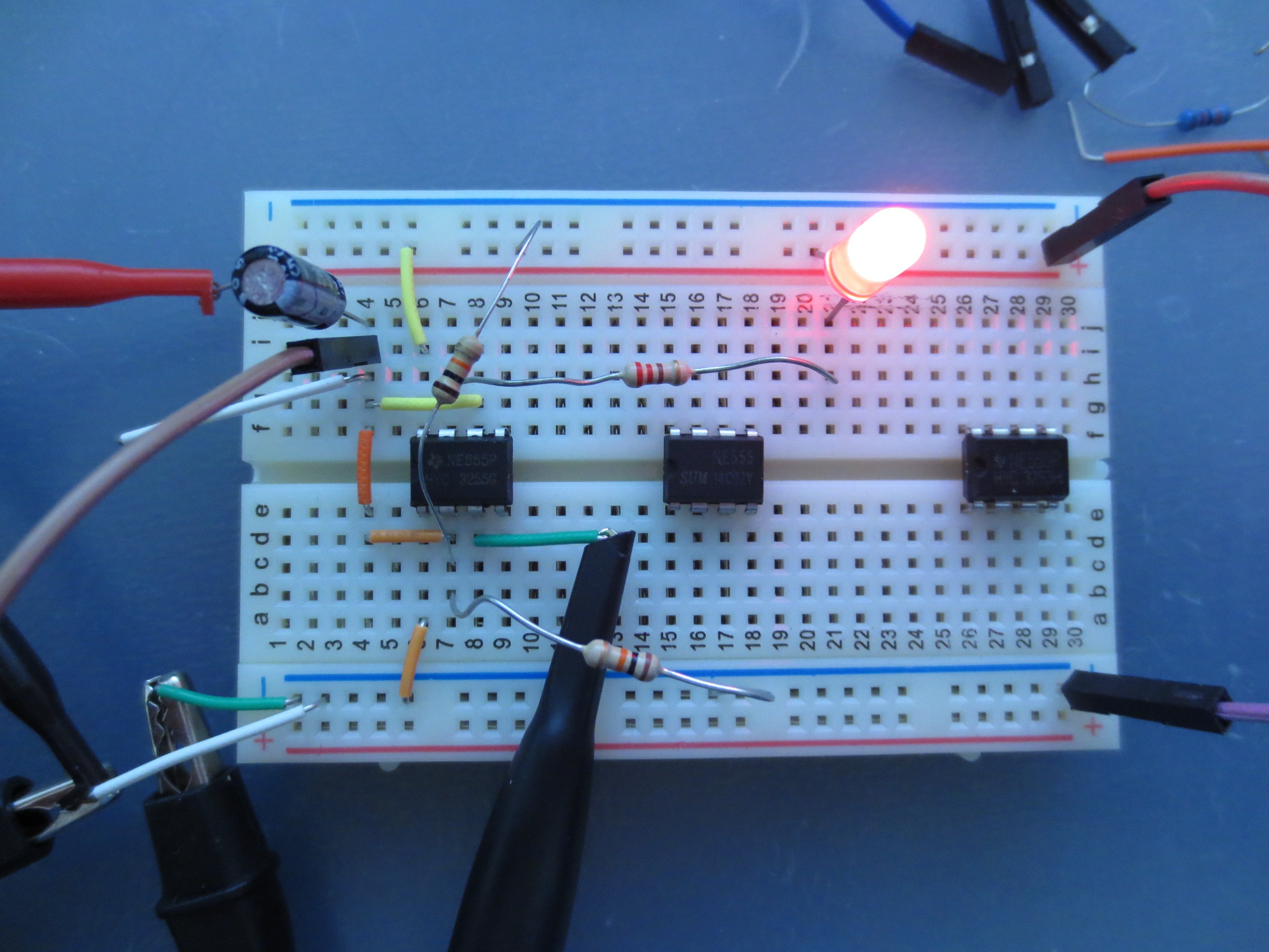
TimIt appears my NE555 are from a few kits I ordered on Aliexpress a while ago. They have some kind of distorted TI logo on them, so I am pretty sure they are not genuine devices, but they should work nevertheless. Time to pull out the breadboard. The resistor capacitor network you can see on the right side is to set the level of my function generator correctly to 0/5V.
Inverter operation
Connecting "TRIG" and "THRS" together allows forming a schmitt-trigger inverter that could serve as a basis for further logic.
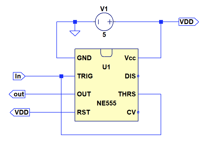
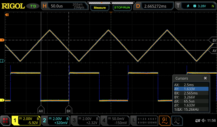
Generally this seems to work very well. See below for a scope image with a triangle at the input, which is converted to a square on the output (channel 1). The threshold levels seem to fit very well too (1/3 VCC and 2/3 VCC, 5V in this case)
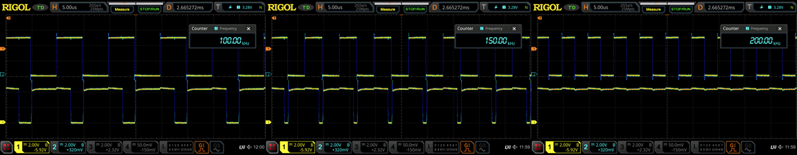
How fast is it? Not very fast, I was only able to achive operation up to 150 kHz with a square input.
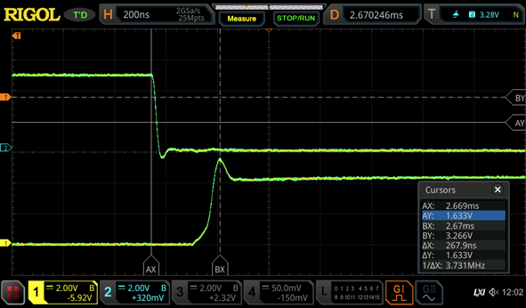
The delay for a low to high transitition seems to be particularily high. I measured between 2.75µs and 3.5µs for the three NE555 that I had.
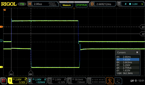
On the other hand, the H->L transition is much faster at 280ns.
Introducing a diode resistor network at the input
Now that we have an operational inverter, we should be able to convert it into a NAND gate by adding a diode-resistor network at the input, as done in diode transistor logic (DTL).
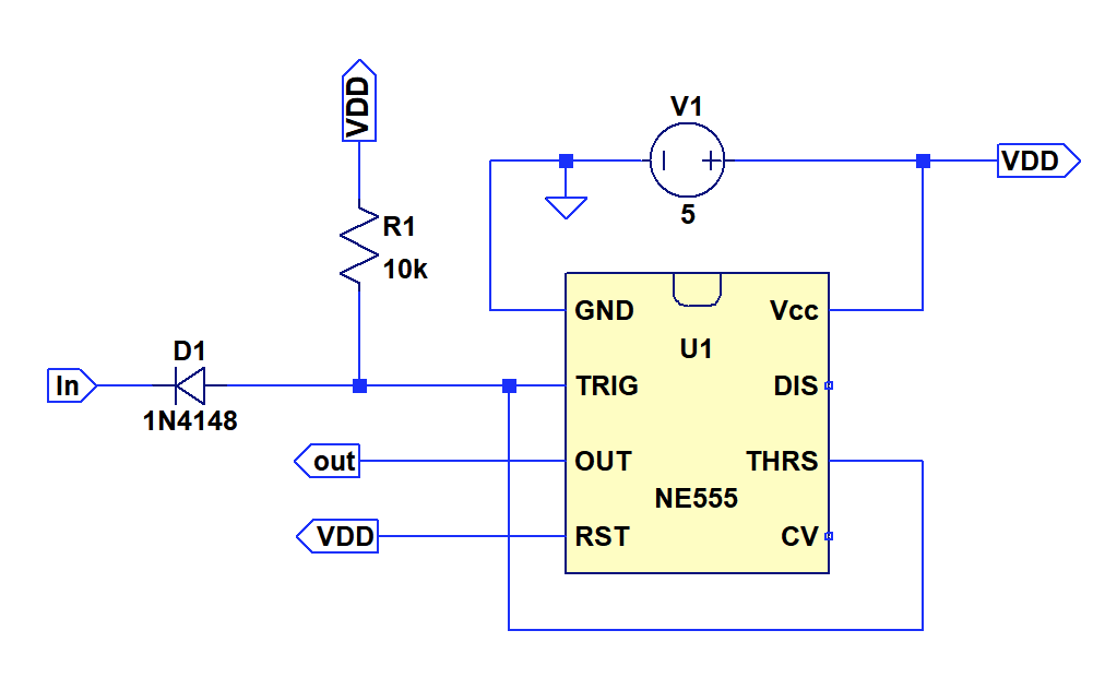
Multiple diodes can be used to add further inputs. The choice of the pull up resistor was rather arbitrary as that was what I found in my parts box, probably a smaller resistor would be a bit better.
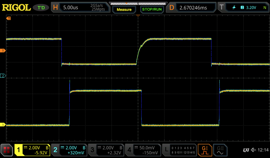
The new contraption works nicely, as seen in the scope picture above. Channel 2 (on top) shows the voltage levels directly at the input of the NE555 (TRIG/THRES). We can see, that the L->H transition at the input is now much slower, since the 10kohm resistor alone as to pull up the node. The H->L transition is fairly quick as the diode has a low impedance.
The inverter still works nicely. Curiously the timing was changed quite significantly to the stand-alone schmitt trigger. The delay fro the L->H transistion on the input is now only 1µs, while the delay for the H->L transition is 1.65µS. The difference is a bit puzzling and understanding it requires digging into the NE555 circuit. But for now it should be fine, NE555-Logic will never be a speed demon anyways.
Conclusions
In conclusion, it appears possible to build inverters and also gates with diode-resistor networks at the inputs. This allows forming NAND2 and NAND3 gates. In addition, we could use the open collector output (DISCH) of the NE555 to form NOR2, NOR3 and AND-OR-INVERTER gates from multiple NE555.
Pretty nice, looks like we got our first toolbox for combinatoric gates together.
Discussions
Become a Hackaday.io Member
Create an account to leave a comment. Already have an account? Log In.