 schlottmachine
The current design uses eight (8) ICs to create the correct signals and change the value of address 1 in a single DMX universe (max 512 addresses or 'channels'). The first timer is in astable mode as an oscillator, triggering the rest of the timers, which are in monostable mode. The output of each timer is coupled to the input to the next using an RC circuit to create a trigger pulse, and all timers are set to count out each part of the data frame - The break signal, Mark After Break (MAB), null start byte, 2 stop bits, start bit, and addr. 1 data byte. Timers which need to manipulate the data bus are connected to an open-collector transistor, and those that simply count out a pulse are daisy-chained to the next timer.
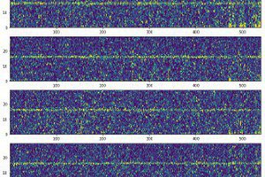
There are two 555s configured as inverters at the end of the chain to clean up the differential signal. You'll notice that the project images show an isolated splitter; this does nothing to change the actual logic of the signal, it only serves to strengthen the data+ and data- signals, as the splitter has RS485 line drivers that do a much better job of driving long runs of cable. The lights in the demo pictures are controlled by a Dove Systems DM-406 shoebox dimmer, which being commercially available, verifies that my 'console' does generate a USITT/ESTA/ANSI compliant DMX512 signal.
The prototype design uses a pot to change the byte as a proof of concept. It loads 1s in from the 'right' of the frame, changing the DMX value between 128 (roughly 50% brightness) and 255 (100% brightness). This is how I actually learned DMX sends data LSb first, not MSb as I assumed. Neat!
The current revision uses BCD switches to select which bits are high or low out of the byte for chan/addr 1. I had trouble with the inter-stage coupling circuits, so only the first three timers are working, and each switches three bits save for the third switch, which does the 7th and 8th bits inclusive of the MSb. It turns lights on and off, though!
 Uri Shaked
 Justin R.
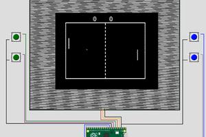
 George Gardner