 Vedran
Intro
This project started as a servo motor tester/driver and eventually turned into a buck converter. I wanted the buck converter to be part of the tester, but since it turned out to be much more complicated than I expected, I decided to give it full attention. So without any further ado...
The goal of this project is to design, build and test a prototype of a buck converter based on NE555. It should be able to take any input voltage higher than desired output, and up to 15V. Output should be adjustable, although the project focuses on a circuit with 5.1V output (strong 5V :D). Choice of output voltage should be easily changed.
Buck converter theory
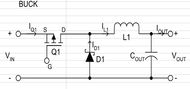
Simplest buck converter normally consists of 2 parts:
- buck stage - doing actual conversion
- driver circuit - usually a clock source, providing a square wave to drive FET(s) in buck stage
Circuit design
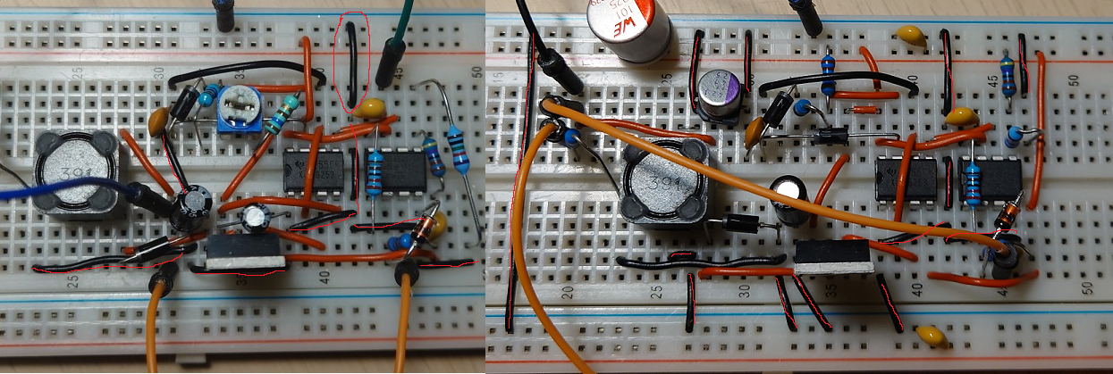
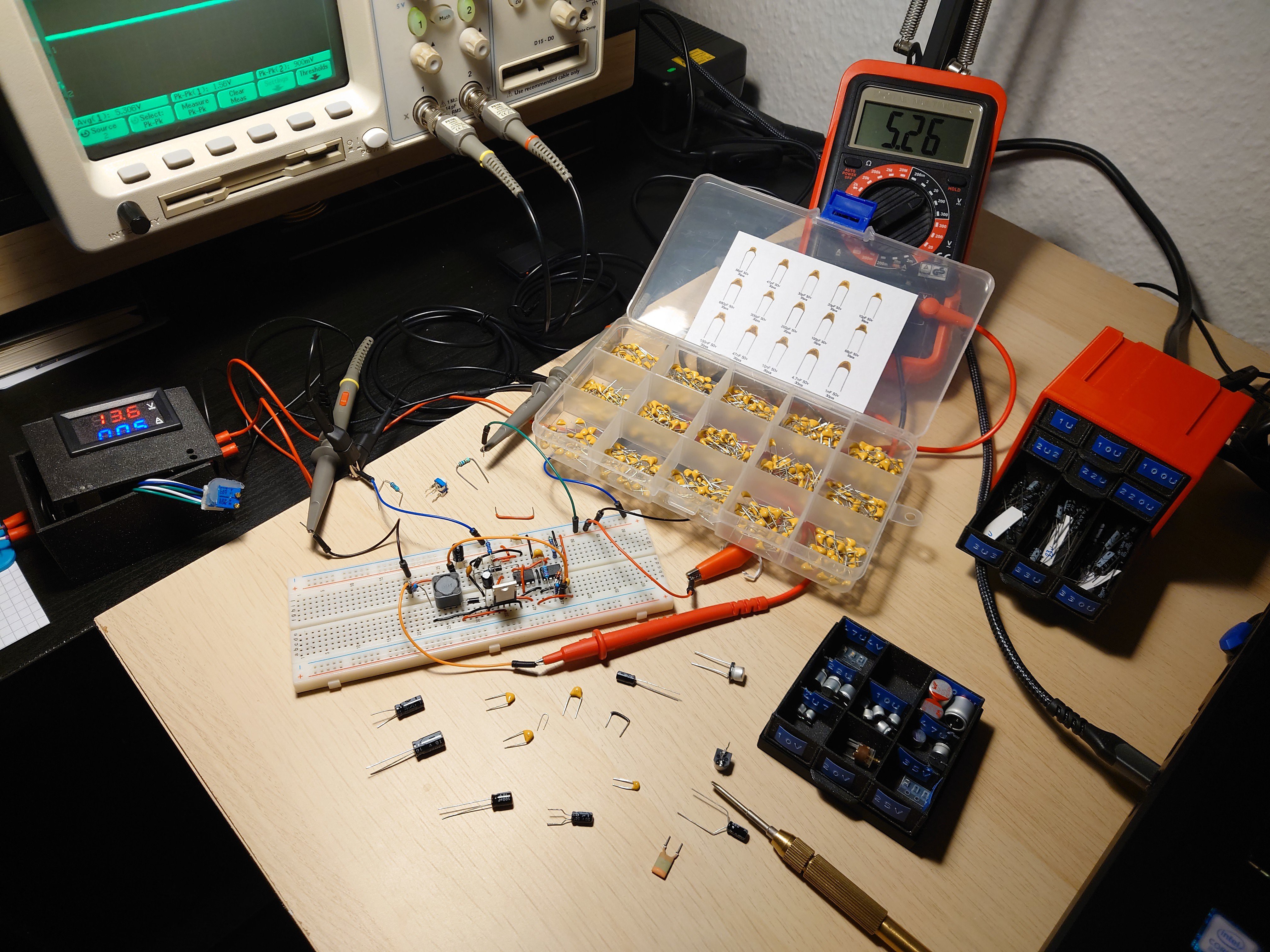
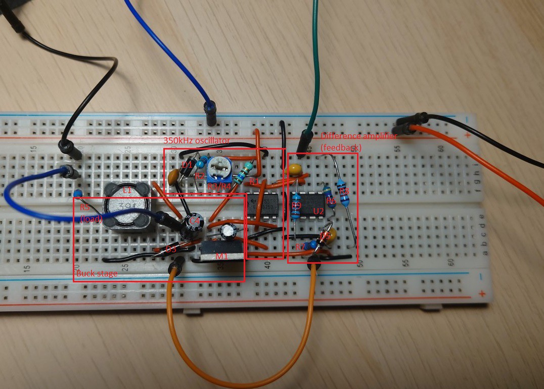
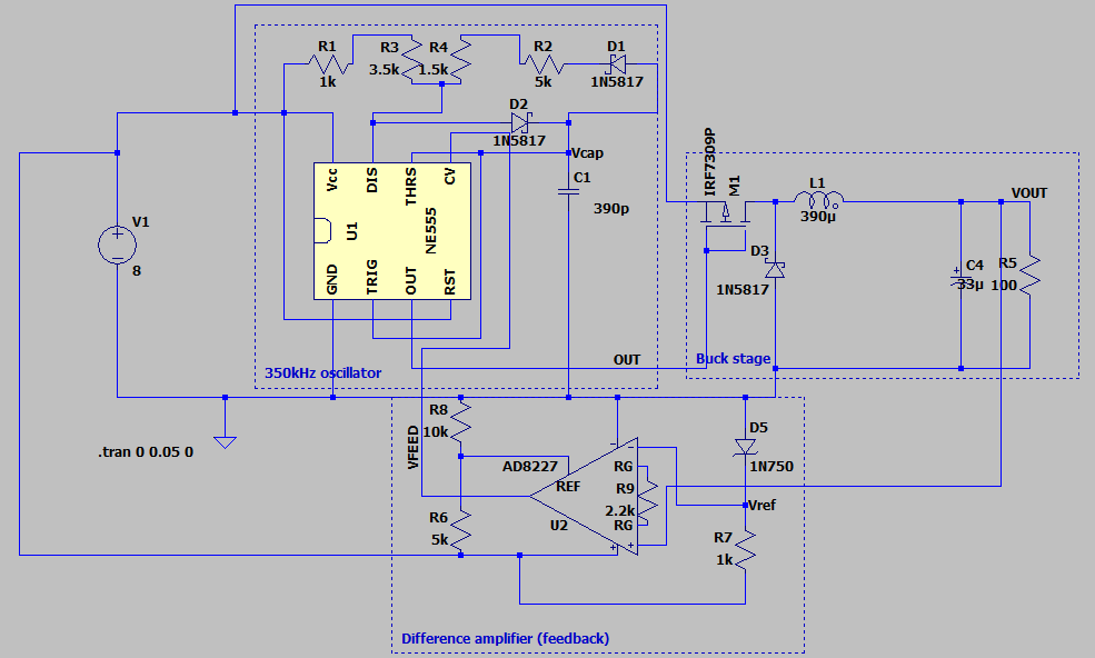
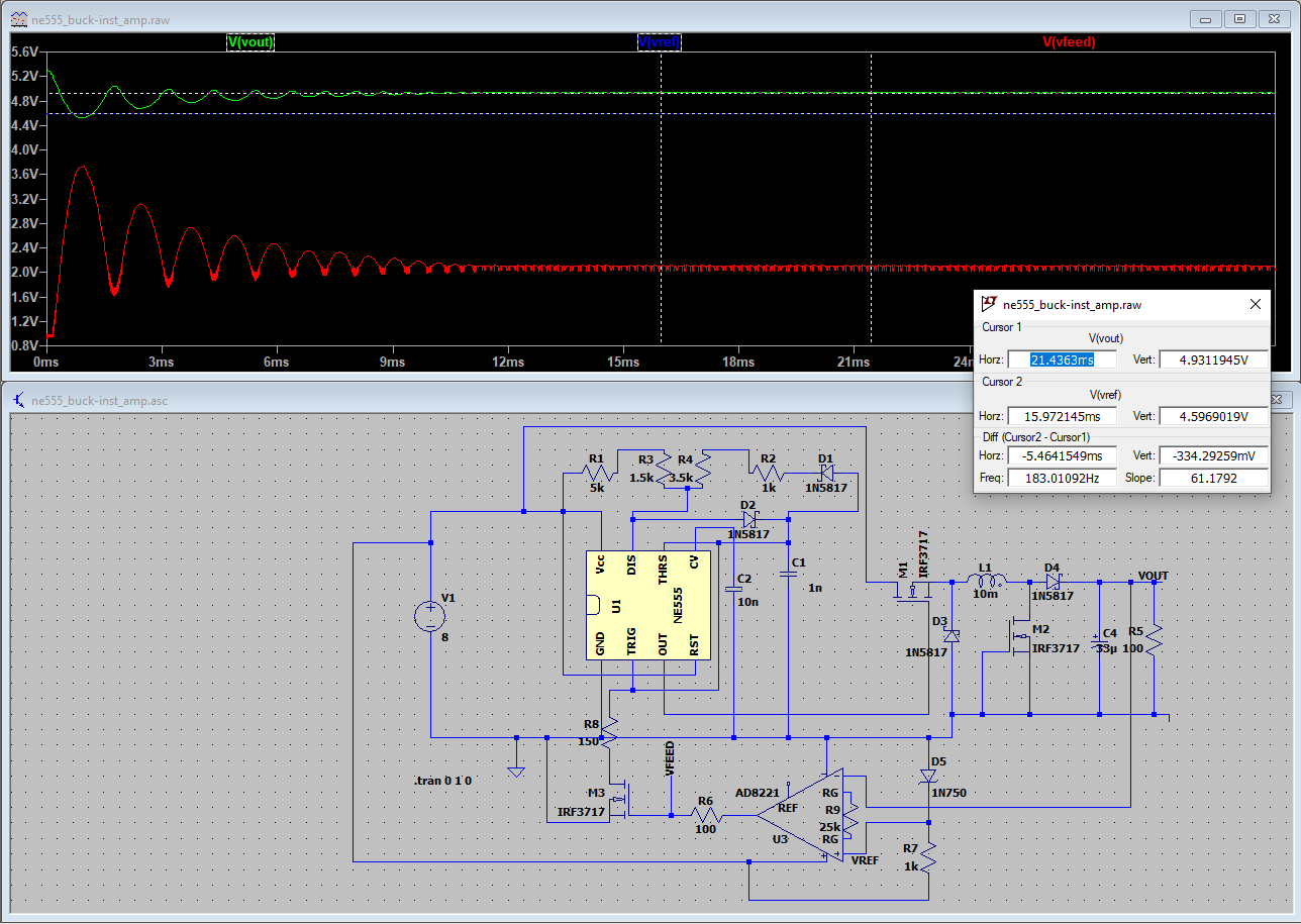
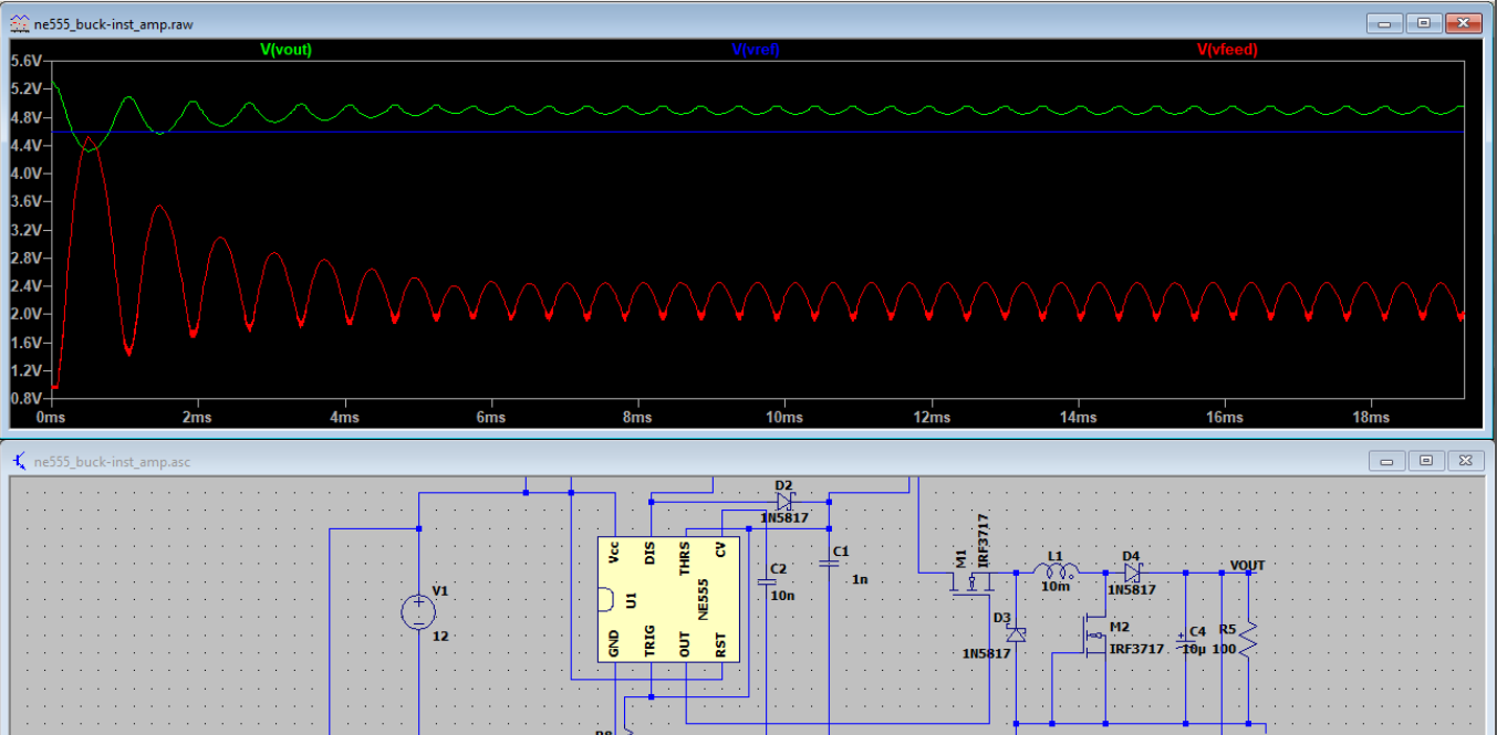
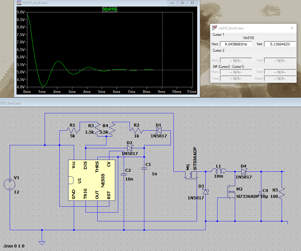
Circuit was designed incrementally (see Logs of this project) as my understanding of a buck converter was very small, and experience of building one even smaller. Initially, a circuit based on the schematic above was made and tested. Once that was tweaked, a feedback loop was added as it was necessary to support a range of input voltages. Eventually, the following was the schematic:
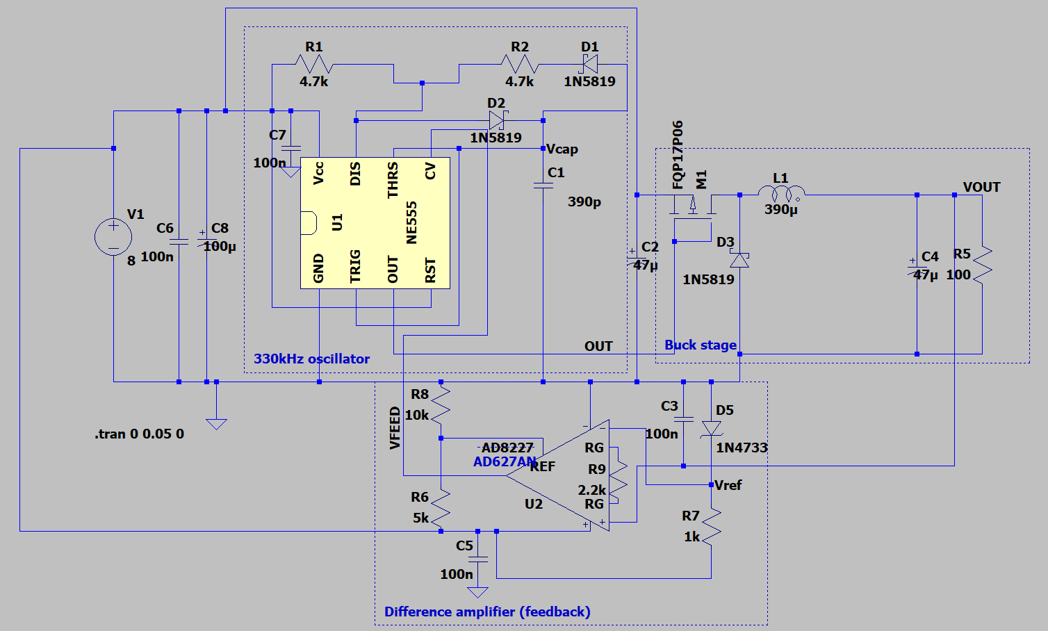
Something that theoretical model above doesn't show is input capacitor(s). Switch mode power supplies need both an input and output capacitors for stable operation. Output capacitor flattens the output voltage and is part of LC resonator. Input capacitor, on the other hand provides a storage close to the converter that's able to quickly discharge to provide current for LC circuit when FET closes. Without it, buck converter would bring down the input supply line sending voltage ripples back into the system.
C6, C8 and C2 play the role of input capacitors, with C6 and C8 being needed because of my voltage source, which is another DC-DC converter with poor output characteristics. With better input, C6 and C8 would not be needed.
I think that even D1 and D2 are no longer needed as duty cycle is preset to 50% and then let to feedback circuit to regulate. Normally, they would allow for altering duty cycle of NE555's output externally.
R5 plays the role of a load, as the circuit output both in reality and in simulation will need some sort of load to settle to a sensible output.
Finally, there's analog feedback circuit based on AD627 instrumentation amplifier. Instrumentation amplifier being a fancy name for amplifier that can take two signals referenced to a common ground, find difference between and potentially amplify them. On top of that, it can in some cases (e.g. here) offer a reference pin. This is useful as one can superimpose input difference onto any thing else. General formula is [Vout] = [Vref] + ( [V+] - [V-] )
Theory of operation
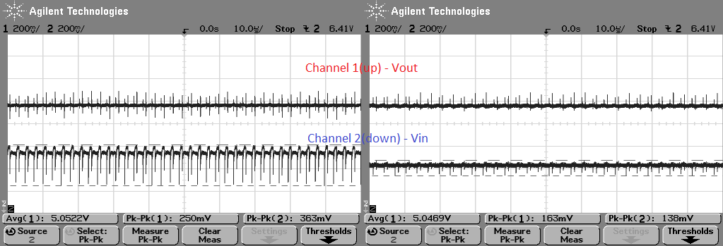
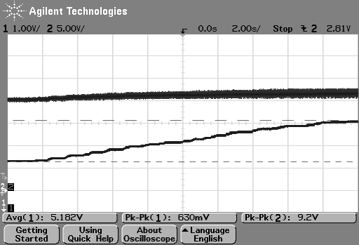
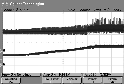
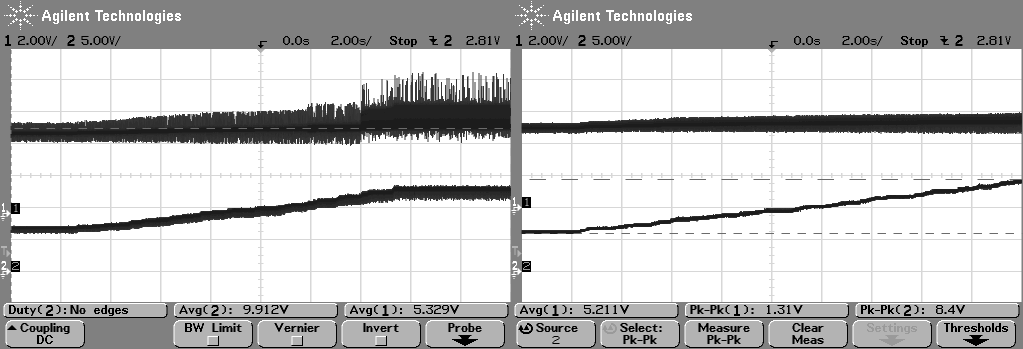
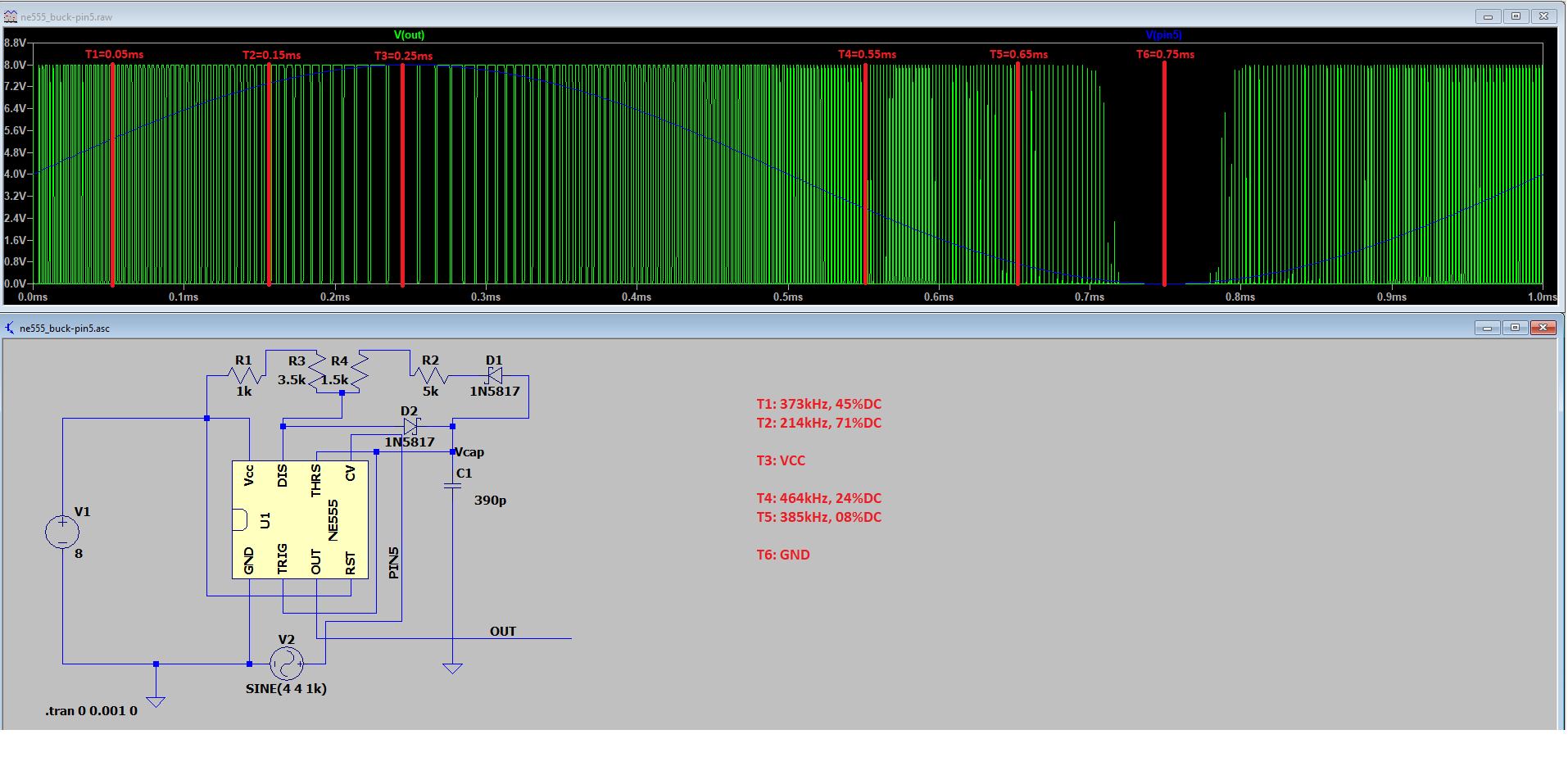
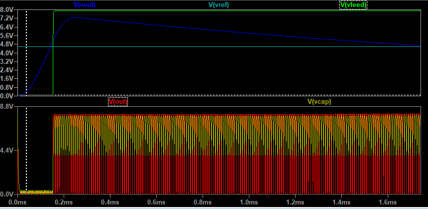
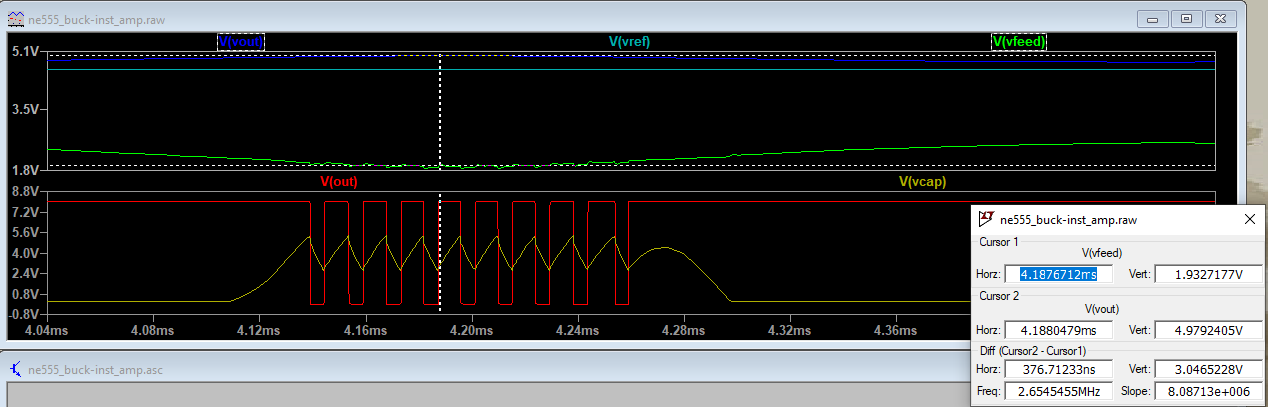
The basic part of operation starts with NE555 producing 50% duty cycle square wave at about 330kHz. This drives the buck stage and which in terms lowers input voltage to something that shows up on Vout. Vout is fed into a feedback amplifier and subtracted from Vref - setpoint that we want the circuit to maintain. Vref is derived with the help of a zener diode to ensure stable reference, independent of input voltage (unlike when using a voltage divider).
Amplifier calculates the difference from the setpoint and adds it to Vref, set to 2/3Vcc via voltage divider. This magic number is chosen as it's normally the threshold which NE555 maintains internally to discharge the timing capacitor (C1) and can be measured on pin 5 when NE555 is powered on. Taking this threshold and adding or subtracting from it difference in output and setpoint allows us to create new threshold that can be fed into NE555. This new threshold is dynamic, varying with buck converter output and can be used to adjust NE555 output - which in term adjust buck converter's...
Read more »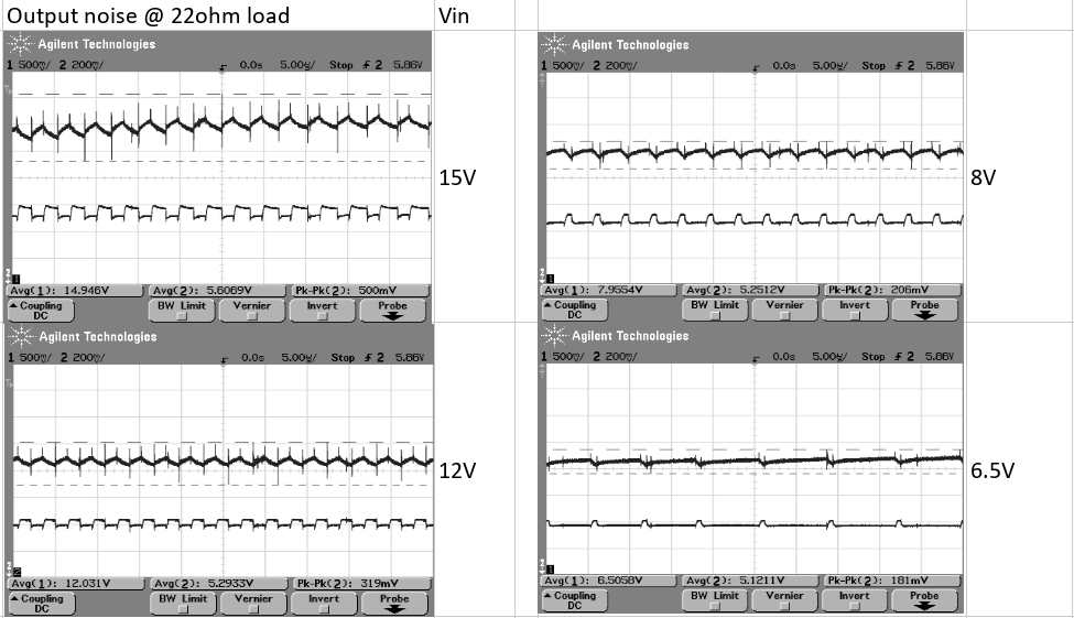


 hesam.moshiri
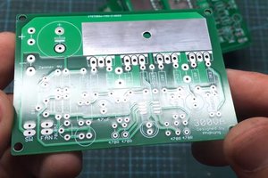
 Electroniclovers123
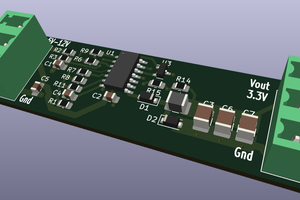
This would work with just a regular op-amp. The operating point would end up being where it needs to be to make the 555 happy. So there's no need for a differential amplifier. The op-amp chosen needs to have no phase reversal and ideally a rail-to-rail input and output.