 Vedran
Day 2 ended with a functional buck converter and a wish to implement feedback so that the converter maintains steady output across a range of inputs. Generally, output voltage of previously made buck converter directly depends on circuit input voltage and the duty cycle (DC) of NE555's output signal:
- increase in DC-> increase in output voltage (with constant input voltage)
- decrease in DC -> decrease in output voltage (with constant input voltage)
- increase input voltage -> increased output voltage (with constant DC)
- decrease input voltage -> decreased output voltage (with constant DC)
In both cases, problem boils down to controlling DC. In the previous circuit, that was controlled by the potentiometer made of R3/R4 that governs charge/discharge interval of capacitor C1. So the problem can be further reduced to controlling the resistance through the two paths:
- charge path: R1 -> R3 -> D2
- discharge path: D1 -> R2 -> R4
With this knowledge, theoretical approach would be to set our threshold (voltage that we want on the output), then compare it to current output voltage, and finally manipulate resistance in one of the paths (e.g. voltage is higher than threshold -> increase the resistance in discharge path) to change output voltage-
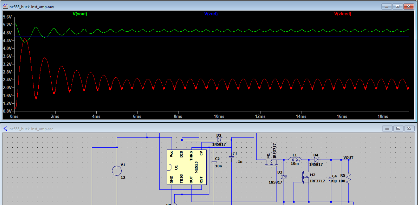
Few iterations got me to a circuit that implements the logic above which I tested in simulation ( with both 12V and 8V input voltage)
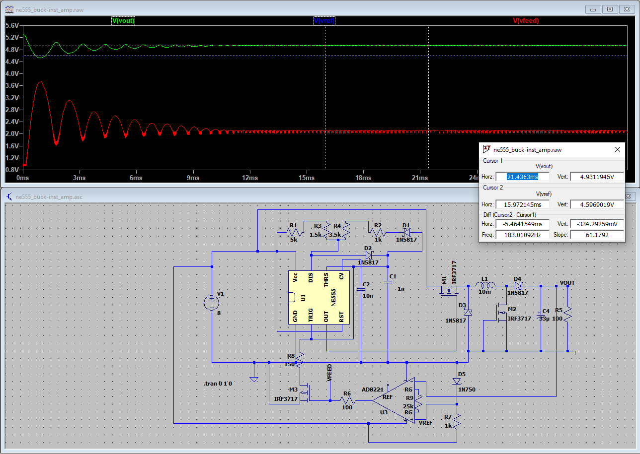
(decreasing C4 at output is here just because i decreases simulation time significantly)
Building up on the circuit from day 2, feedback is taken from output and passed into the instrumentation amplifier to be compared with reference voltage. Ideally, reference voltage is what we'd like to get at the output.
Reference
Reference voltage is derived with a help of zener diode, to allow for flexible input voltage (this simulation uses reference of 4.6V, in reality, this well be slightly above 5V). This reference and buck output are then fed into the instrumentation amplifier with gain 3, such that every difference between output voltage an the reference is tripled on the output.
Additional path
Amplifier output (Vref above) is used to drive N-FET connecting C1 to the ground over 150ohm resistor. This provides an additional discharge path for the C1 that can be activated independent of discharge pin on NE555.
Operation principle
Originally, I arrived to this circuit following the idea from above, trying to manipulate resistance of discharge path for C1 capacitor.
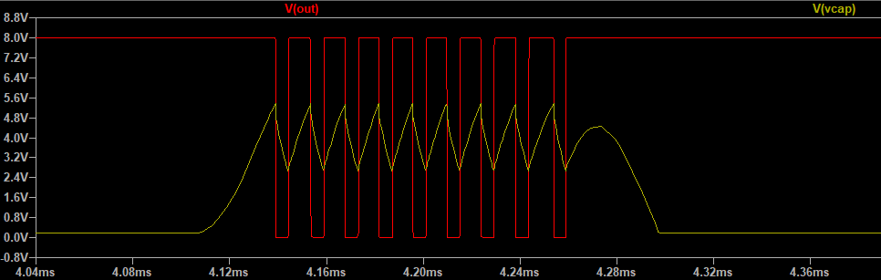
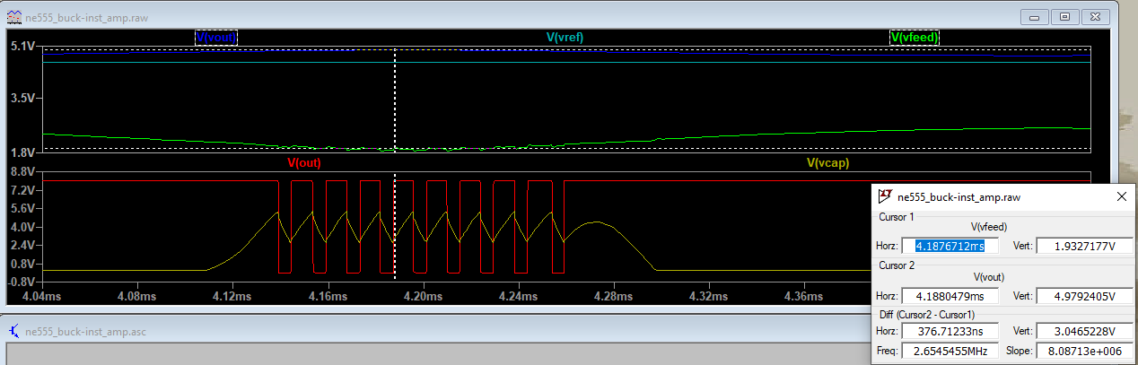
I now realize that I got what looks the be desired outcome, but the principle of work is different. C1 is most often discharged only through FET, as FET gets to open independent of the discharge pin on NE555 (seen in the last bump). In doing so, we do not manipulate total resistance of discharge path, but instead provide an additional discharge path outside of charge/discharge cycle governed by NE555. The problem I can see here is that when FET opens and essentially shorts C1 to GND, NE555 output is pulled high. This in term causes buck output to raise, which through feedback and amplifier should increase the output of the amplifier, driving the FET to close even more and keep C1 shorted.
But it still works?
Apparently, but I think it's because I messed up the wiring and swapped the inputs on amplifier. So as the output voltage nears the reference, amplifier output grows and vice versa.
I think I'll give this another go with lessons learned...
Discussions
Become a Hackaday.io Member
Create an account to leave a comment. Already have an account? Log In.