 Vedran
I finished earlier post with an idea to implement feedback by manipulating charge/discharge path resistance and in the way change duty cycle of NE555 output. Several attempts at this over the holidays failed miserably in one of the following ways:
- output locks up in high state if the difference between output and threshold is too high
- when the system is tweaked to one input voltage (e.g. 8V), timings and everything change as soon as input voltage is changed
It became clear that I needed a different approach. At this point, I was ready to give up an actual buck-converter with very stable 5V output, and settle for something that at least resembles a buck converter, i.e. output voltage is reduced, and doesn't vary outside of input spec of of a typical servo motor (4.8V - 6.5V) over an input range of 5V - 12V. Desperate, I know.
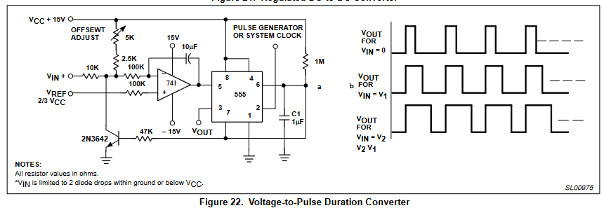
While reading for this project, I came across an interesting application note that showed a circuit labeled "Voltage-to-pulse duration circuit", and I got inspired.
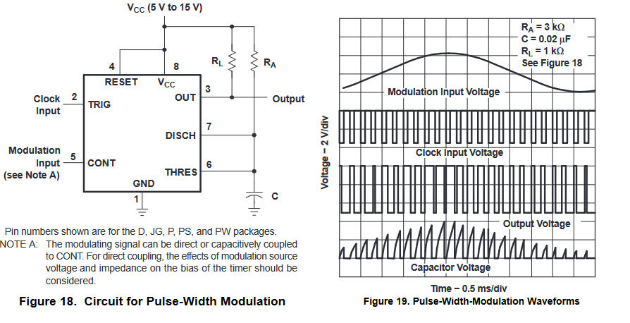
The mystery of pin 5
The circuit is relying on supplying feedback through an opamp into pin 5 of NE555. This was the first time I saw anything apart from 10n capacitor connected to pin 5. Looking further into the NE555 datasheet, pin 5 can also be used for modulation where change in voltage on pin 5 changes charge discharge limits of the timing capacitor.
So I ran a simulation on a simplified NE555 circuit I am planning to use, with a voltage on pin 5 from 0 to Vcc.
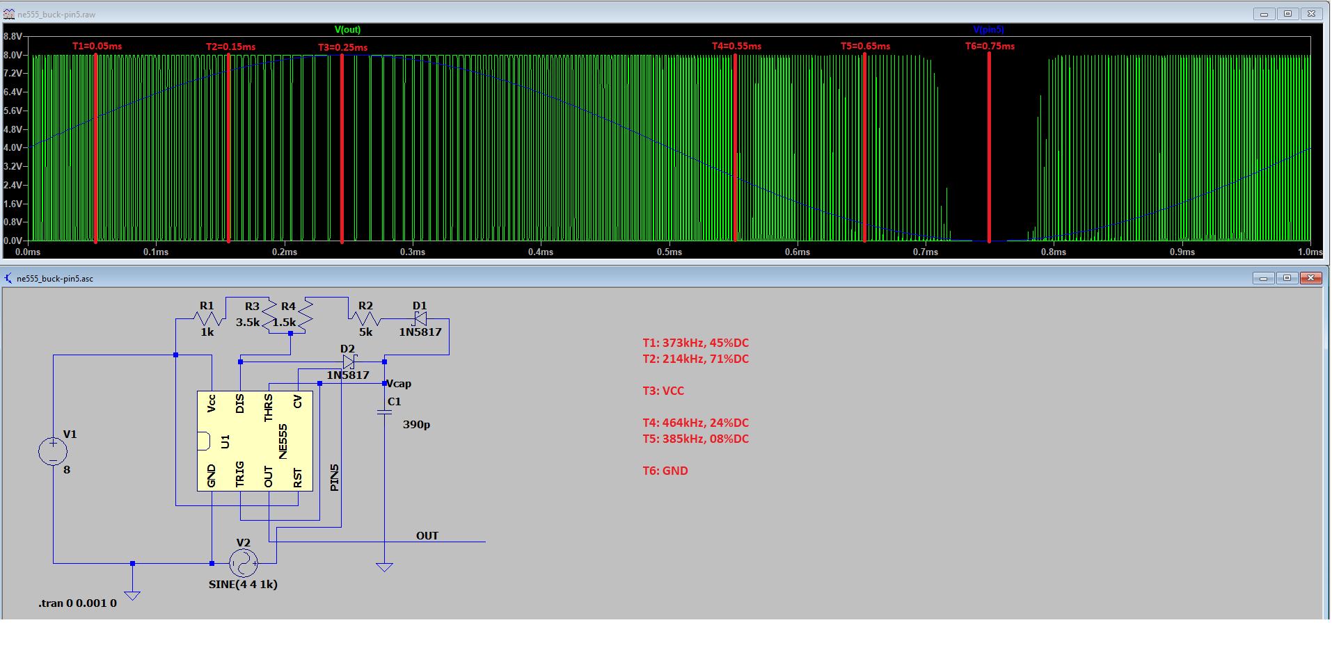
What follows is that by increasing voltage on pin 5, output frequency (pin 3) decreases, while the duty cycle increases until V(pin5) = Vcc, and duty cycle is 100%. And vice-versa, by lowering the voltage, frequency increases while duty cycle drops until it reaches 0% and output is brought to GND.
To understand what governs this behavior, we look at internal components comprising NE555. From the application note above, it's visible that pin 5 can supply reference voltage into comparators that control when timing capacitor charges and discharges. Left untouched, it ensures there's (1/3)Vcc and (2/3)Vcc references present on the internal comparators.
And so, the first prototype
With everything learned so far, I put together the prototype below
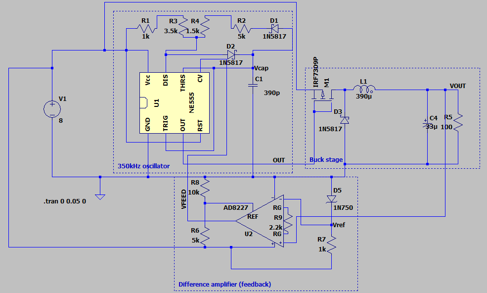
Oscillator
Same oscillator as in the examples before. Designed to produce 350kHz square wave with duty cycle from one of the first working models with no feedback and 12V input. Potentially tweaked in the future to different DC.
Buck stage
Same buck stage as mentioned before, roughly estimated using a calculator provided by Texas Instruments for designing buck convertor stages. I did some compromises on the numbers returned by the calculator to be able to build the converter with the parts I have available. 100 ohm R5 simulates load on at the output. One notable change from older designs is a change to P-channel FET, as I noticed N-FET would lock up in open state, making the circuit settle on 0V output, and NE555 output 0V at the same time. To account for P-FET instead of N-FET, values of R1 and R2 as well as R3 and R4 are swapped as charge-discharge curve now triggers FET on opposite polarities.
Difference amplifier (feedback)
Instrumentation amplifier is used to calculate the difference between output voltage of the circuit and the 5V reference, amplify it feed it out to the NE555 with one catch. NE555 has previously been designed with no voltage applied on pin 5 (see earlier designs). As discussed previously, no voltage means (2/3)Vcc so the amplifier output if offset by (2/3)Vcc and any error between Vout and Vref is then added or subtracted from the reference.
All that's left is run the simulation an confirm everything is as it should be
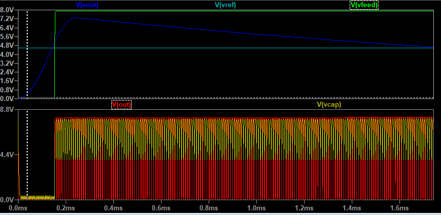
Well, almost. Everything seems to go smooth, and as expected, until Vout finally hits Vref. At that point simulation apparently becomes too complex and during the last 10h of simulating, I did not come past 1.8ms. Looks like its, time to build the circuit :)
Discussions
Become a Hackaday.io Member
Create an account to leave a comment. Already have an account? Log In.