 Vedran
Second round of optimization started with tiding up the wiring a bit and surprised me with a discovery that my grounding in the circuit was rather poor. I tried to tie all contacts over a single ground bus through my circuit, instead of going out to ground rail (left).
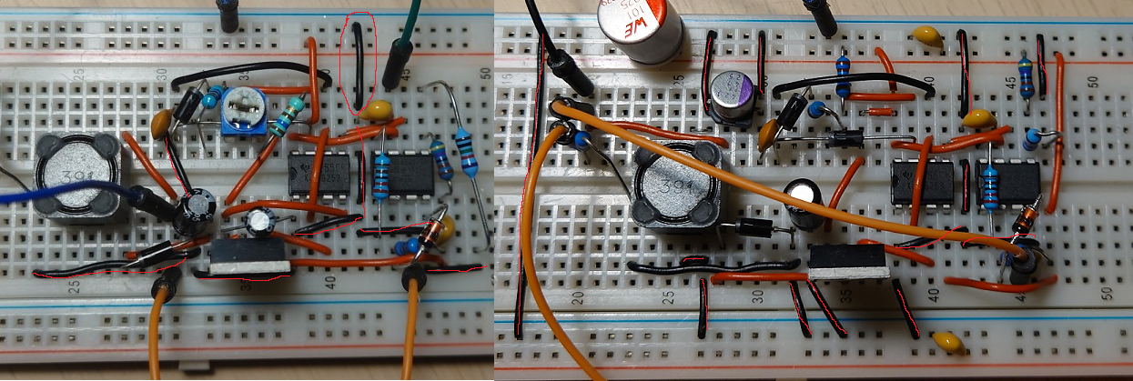
New circuit has a lot more ground connections out to the rails. (right) I have also added a couple of dummy GND connection (bottom part of the right figure), hoping to create a ground plane around the FET and inductor to reduce the noise. There's some drop in noise after introducing these GND wires around, but given the janky breadboard setup, its within the measuring error.
Finally, one more aluminum input capacitor (100u) was added directly to rail and few 10n/100n sprinkled around the breadboard to shave off some 200mV of noise on input.
In addition, I have also tried to tidy up the circuit a bit, rewiring some things, shortening some of the components legs and removing unnecessary components. In that process, I removed the potentiometer and 2 surrounding resistors, replacing them with 4.7k resistor on each side, giving the circuit new frequency of ~330kHz.
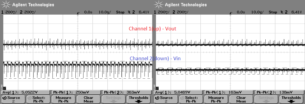
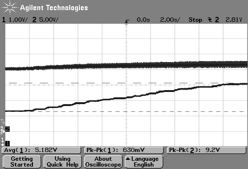
With all the, I got to about as good as I think I can. Output noise is some 70mV over input noise and output voltage varies about 200mV over the range of 6.5V to 15V. I should also probably mention that my voltage source is not ideal as it's made out of a cheap DC-DC converter and has ~200mV of noise on the output. (you can catch a glimpse of it in Optimization part 1)
Final result is below
Discussions
Become a Hackaday.io Member
Create an account to leave a comment. Already have an account? Log In.