Vedran
-
Tests
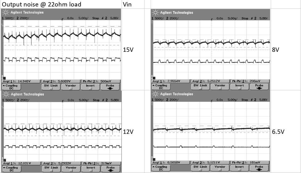
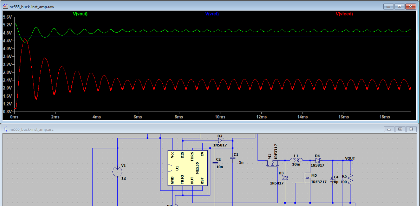
01/09/2022 at 14:30 • 0 commentsTo summarize the project, I wanted to do some characterization of the converter. Mostly noise and in/out power (efficiency) measured over a shunt resistor.
Noise
![]()
Comparison of noise/ripple on output signal (channel 2, top) at different input voltages (channel 1, bottom) Efficiency
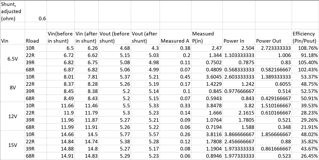
Efficiency was calculated by adding 2 shunt resistors to the circuit - one on the input and one at the output. Current was then calculated by measuring voltage drop over them, multiplied with the voltage directly after resistor to get power getting into the circuit and out of it.
Dividing output power with input power should produce efficiency. I also did measurements for 4 different input voltages and 4 different resistive loads.
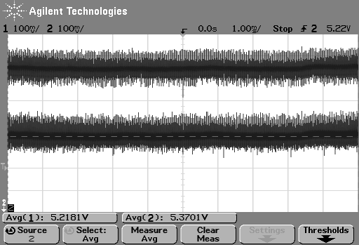
Voltage drop was measured by connecting two oscilloscope probes - one before shunt, one after shunt. Scope was set 100mV/division for each probe, with sampling time of 10ms over which the average voltage was computed.
![]()
Current measurement example showing voltage before shunt (channel 2) and after (channel 1)
Measuring current/efficiency doesn't really make sense to do on a breadboard where the traces/connections itself could produce higher resistivity than a shunt resistor. And as my measurements show, it really is all over the place - nevertheless it was fun to try at least.![]()
Efficiency estimates My shunt is 0.05mOhm in reality, but I had to adjust its value in calculations to attempt matching the power output my power supply claimed was being outputted - so it's now at about 0.6ohm instead.
Column Measured A is current reported by my power supply (probably not trustworthy measurement either), and Measured P(in) calculates power delivered on input by multiplying Vin (before in shunt) and Measured A.
All this leads to some fun results, +100% efficiency (yay, free energy!). In all seriousness, these numbers in the sheet above are not to be trusted and measurements should be repeated on a built circuit.
-
Optimization part 2
01/09/2022 at 00:24 • 0 commentsSecond round of optimization started with tiding up the wiring a bit and surprised me with a discovery that my grounding in the circuit was rather poor. I tried to tie all contacts over a single ground bus through my circuit, instead of going out to ground rail (left).
![]()
Grounding before (left) and after (right) New circuit has a lot more ground connections out to the rails. (right) I have also added a couple of dummy GND connection (bottom part of the right figure), hoping to create a ground plane around the FET and inductor to reduce the noise. There's some drop in noise after introducing these GND wires around, but given the janky breadboard setup, its within the measuring error.
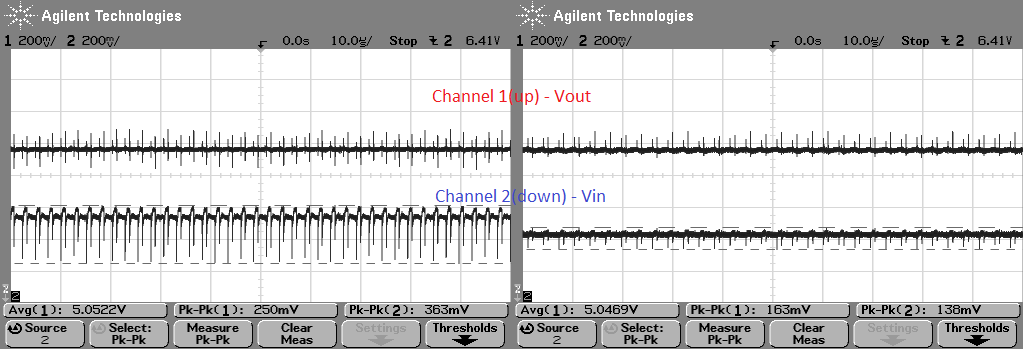
Finally, one more aluminum input capacitor (100u) was added directly to rail and few 10n/100n sprinkled around the breadboard to shave off some 200mV of noise on input.
![]()
Noise on input (channel 2, bottom) and output(channel 1, top) before (left) after (right) additional capacitors In addition, I have also tried to tidy up the circuit a bit, rewiring some things, shortening some of the components legs and removing unnecessary components. In that process, I removed the potentiometer and 2 surrounding resistors, replacing them with 4.7k resistor on each side, giving the circuit new frequency of ~330kHz.
With all the, I got to about as good as I think I can. Output noise is some 70mV over input noise and output voltage varies about 200mV over the range of 6.5V to 15V. I should also probably mention that my voltage source is not ideal as it's made out of a cheap DC-DC converter and has ~200mV of noise on the output. (you can catch a glimpse of it in Optimization part 1)
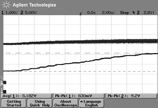
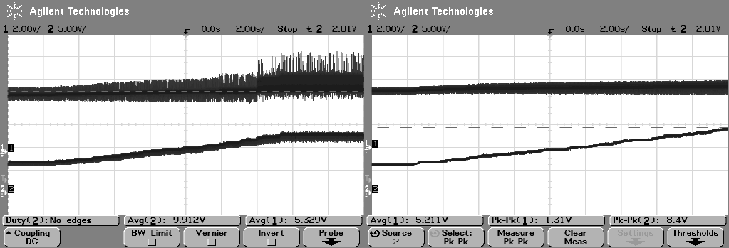
Final result is below
![]()
Output voltage (channel 1, top) hovering around 5.1V as input voltage (channel 2, bottom) increases from 6.5V to ~15V -
Optimization part 1
01/08/2022 at 20:34 • 0 commentsThe circuit kinda works, but it leaves a lot to be desired. There's 3 areas that I'd like to improve:
- Input - catches a lot of switching noise going from around ##V (nothing connected) to over 3Vpp once buck converter goes berzerk, around 11V input
- Output ripple - it’s too unstable to be called buck converter. There’s 2.5V of ripple present on the output measurements
- Output floating with input voltage - currently, output will float for about 0.5V when input voltage changes from 6V to 12V. Ideally, there should be no floating
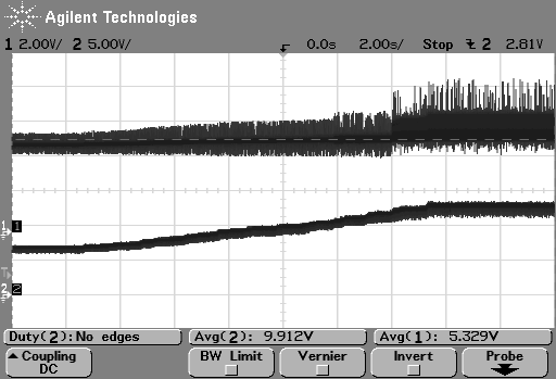
![]()
Baseline; Output (channel 1, top) trying to keep up with 5.1V reference as the input (channel2, bottom) increases from 6.5V to ~12V Capacitances
I think the part where I can improve the most is tweaking input/output capacitances. So I grabbed all of my capacitors and started playing around.
![]()
Currently, my physical circuit features only one 10uF input capacitor and one output 33uF capacitor. So I set input voltage to 13V (well in the region where ripple is high) and started testing different capacitors. Trial an error (table below) gave 47u as the best available option.
Input ripple (VinPP) Output ripple (VoutPP) Input capacitance (Cin) 3.4V 1.4V 10u 1.5V 0.9V 22u 1.7V 0.9V 33u 1.4V 0.9V 47u 1.8V 0.9V 100u Or graphically
![]()
Noise on the output (channel 1, top) as the input voltage (channel 2, bottom) changes from 6.5V to 12V -
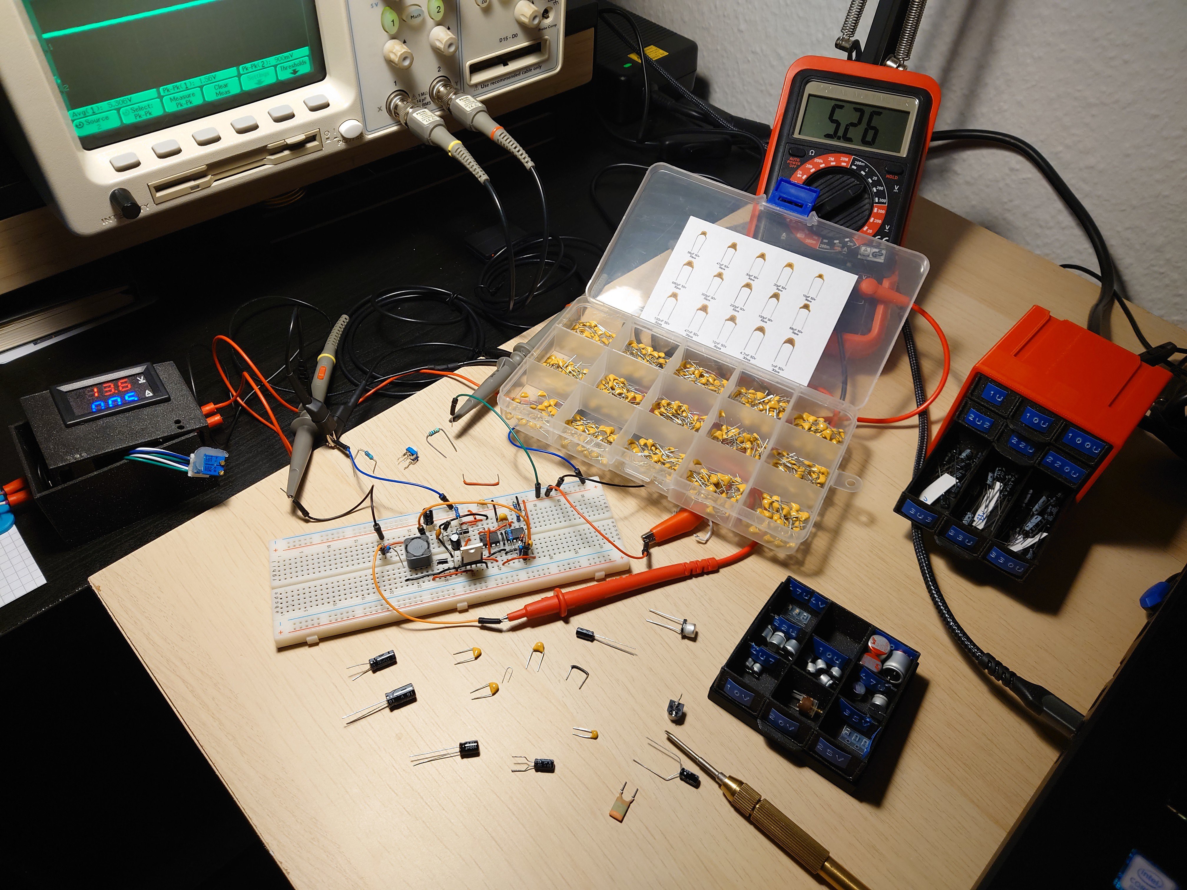
First prototype
01/08/2022 at 12:19 • 0 comments![]()
First breadboard prototype matching different parts of the circuit to schematics First prototype has now been put together and the result don't look too bad. Measuring output while the input voltage is being adjusted from 6V to 12V produces between 5V and 5.5V output., with a lot of noise as the input voltage increases.
![]()
Output (channel 1, top) trying to keep up with 5.1V reference as the input (channel 2, bottom) increases from 6.5V to ~12V It's not the best converter yet, but, in principle, it does what it's supposed to ^^ There's room for improvements...
-
First working model
01/05/2022 at 17:09 • 0 commentsI finished earlier post with an idea to implement feedback by manipulating charge/discharge path resistance and in the way change duty cycle of NE555 output. Several attempts at this over the holidays failed miserably in one of the following ways:
- output locks up in high state if the difference between output and threshold is too high
- when the system is tweaked to one input voltage (e.g. 8V), timings and everything change as soon as input voltage is changed
It became clear that I needed a different approach. At this point, I was ready to give up an actual buck-converter with very stable 5V output, and settle for something that at least resembles a buck converter, i.e. output voltage is reduced, and doesn't vary outside of input spec of of a typical servo motor (4.8V - 6.5V) over an input range of 5V - 12V. Desperate, I know.
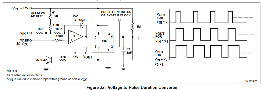
While reading for this project, I came across an interesting application note that showed a circuit labeled "Voltage-to-pulse duration circuit", and I got inspired.
![]()
source: https://www.555-timer-circuits.com/datasheets/555an.pdf The mystery of pin 5
The circuit is relying on supplying feedback through an opamp into pin 5 of NE555. This was the first time I saw anything apart from 10n capacitor connected to pin 5. Looking further into the NE555 datasheet, pin 5 can also be used for modulation where change in voltage on pin 5 changes charge discharge limits of the timing capacitor.
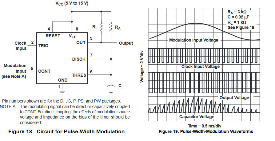
![]()
source: https://www.ti.com/lit/ds/symlink/ne555.pdf So I ran a simulation on a simplified NE555 circuit I am planning to use, with a voltage on pin 5 from 0 to Vcc.
![]()
What follows is that by increasing voltage on pin 5, output frequency (pin 3) decreases, while the duty cycle increases until V(pin5) = Vcc, and duty cycle is 100%. And vice-versa, by lowering the voltage, frequency increases while duty cycle drops until it reaches 0% and output is brought to GND.
To understand what governs this behavior, we look at internal components comprising NE555. From the application note above, it's visible that pin 5 can supply reference voltage into comparators that control when timing capacitor charges and discharges. Left untouched, it ensures there's (1/3)Vcc and (2/3)Vcc references present on the internal comparators.
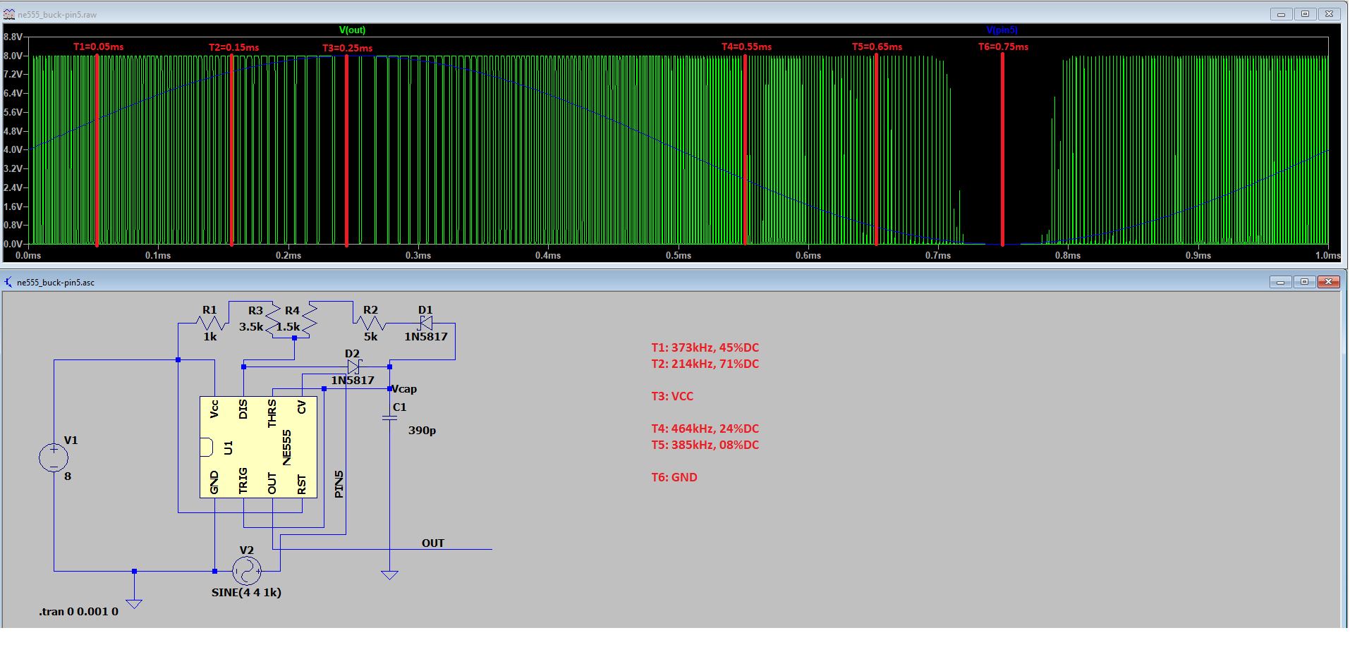
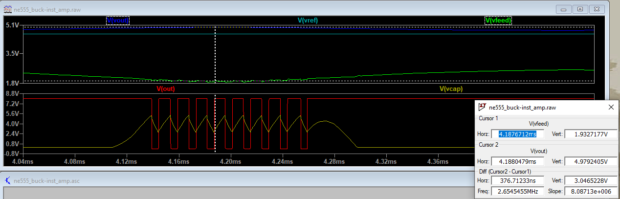
And so, the first prototype
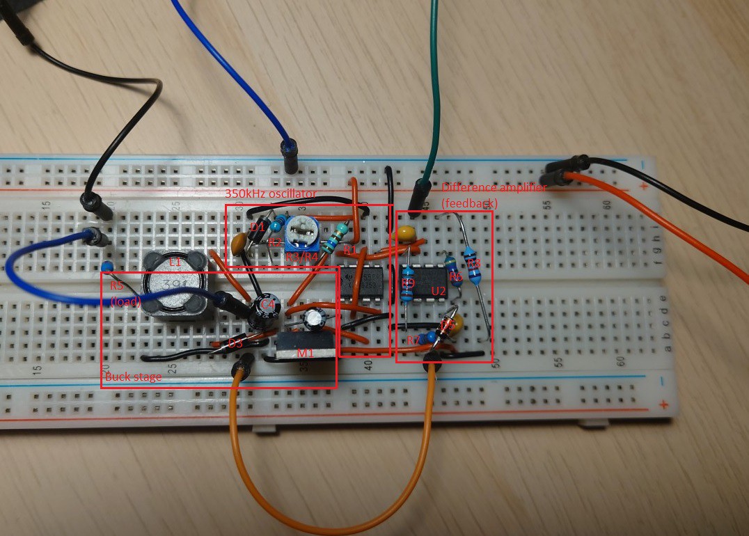
With everything learned so far, I put together the prototype below
![]()
Oscillator
Same oscillator as in the examples before. Designed to produce 350kHz square wave with duty cycle from one of the first working models with no feedback and 12V input. Potentially tweaked in the future to different DC.
Buck stage
Same buck stage as mentioned before, roughly estimated using a calculator provided by Texas Instruments for designing buck convertor stages. I did some compromises on the numbers returned by the calculator to be able to build the converter with the parts I have available. 100 ohm R5 simulates load on at the output. One notable change from older designs is a change to P-channel FET, as I noticed N-FET would lock up in open state, making the circuit settle on 0V output, and NE555 output 0V at the same time. To account for P-FET instead of N-FET, values of R1 and R2 as well as R3 and R4 are swapped as charge-discharge curve now triggers FET on opposite polarities.
Difference amplifier (feedback)
Instrumentation amplifier is used to calculate the difference between output voltage of the circuit and the 5V reference, amplify it feed it out to the NE555 with one catch. NE555 has previously been designed with no voltage applied on pin 5 (see earlier designs). As discussed previously, no voltage means (2/3)Vcc so the amplifier output if offset by (2/3)Vcc and any error between Vout and Vref is then added or subtracted from the reference.
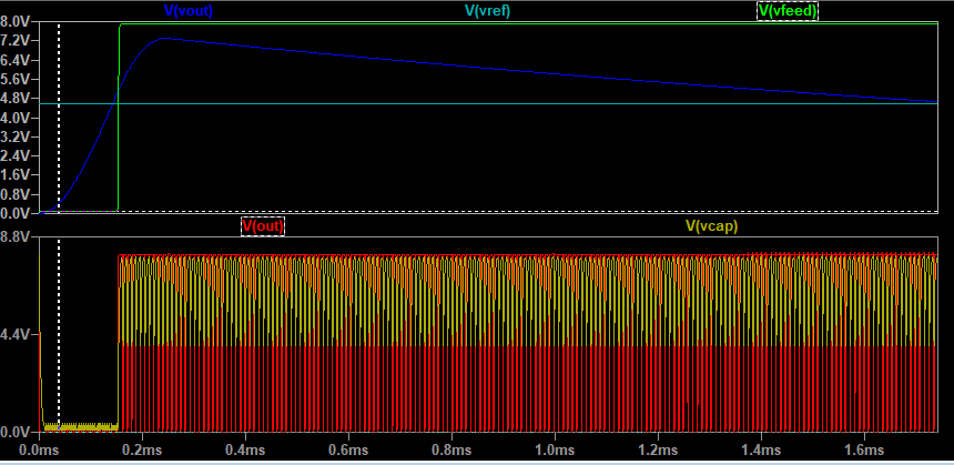
All that's left is run the simulation an confirm everything is as it should be
![]()
Well, almost. Everything seems to go smooth, and as expected, until Vout finally hits Vref. At that point simulation apparently becomes too complex and during the last 10h of simulating, I did not come past 1.8ms. Looks like its, time to build the circuit :)
-
Day 3: Feedback loop
12/19/2021 at 08:46 • 0 commentsDay 2 ended with a functional buck converter and a wish to implement feedback so that the converter maintains steady output across a range of inputs. Generally, output voltage of previously made buck converter directly depends on circuit input voltage and the duty cycle (DC) of NE555's output signal:
- increase in DC-> increase in output voltage (with constant input voltage)
- decrease in DC -> decrease in output voltage (with constant input voltage)
- increase input voltage -> increased output voltage (with constant DC)
- decrease input voltage -> decreased output voltage (with constant DC)
In both cases, problem boils down to controlling DC. In the previous circuit, that was controlled by the potentiometer made of R3/R4 that governs charge/discharge interval of capacitor C1. So the problem can be further reduced to controlling the resistance through the two paths:
- charge path: R1 -> R3 -> D2
- discharge path: D1 -> R2 -> R4
With this knowledge, theoretical approach would be to set our threshold (voltage that we want on the output), then compare it to current output voltage, and finally manipulate resistance in one of the paths (e.g. voltage is higher than threshold -> increase the resistance in discharge path) to change output voltage-
Few iterations got me to a circuit that implements the logic above which I tested in simulation ( with both 12V and 8V input voltage)
![]()
![]()
(decreasing C4 at output is here just because i decreases simulation time significantly)
Building up on the circuit from day 2, feedback is taken from output and passed into the instrumentation amplifier to be compared with reference voltage. Ideally, reference voltage is what we'd like to get at the output.
Reference
Reference voltage is derived with a help of zener diode, to allow for flexible input voltage (this simulation uses reference of 4.6V, in reality, this well be slightly above 5V). This reference and buck output are then fed into the instrumentation amplifier with gain 3, such that every difference between output voltage an the reference is tripled on the output.
Additional path
Amplifier output (Vref above) is used to drive N-FET connecting C1 to the ground over 150ohm resistor. This provides an additional discharge path for the C1 that can be activated independent of discharge pin on NE555.
Operation principle
Originally, I arrived to this circuit following the idea from above, trying to manipulate resistance of discharge path for C1 capacitor.
![]()
I now realize that I got what looks the be desired outcome, but the principle of work is different. C1 is most often discharged only through FET, as FET gets to open independent of the discharge pin on NE555 (seen in the last bump). In doing so, we do not manipulate total resistance of discharge path, but instead provide an additional discharge path outside of charge/discharge cycle governed by NE555. The problem I can see here is that when FET opens and essentially shorts C1 to GND, NE555 output is pulled high. This in term causes buck output to raise, which through feedback and amplifier should increase the output of the amplifier, driving the FET to close even more and keep C1 shorted.
But it still works?
Apparently, but I think it's because I messed up the wiring and swapped the inputs on amplifier. So as the output voltage nears the reference, amplifier output grows and vice versa.
![]()
I think I'll give this another go with lessons learned...
-
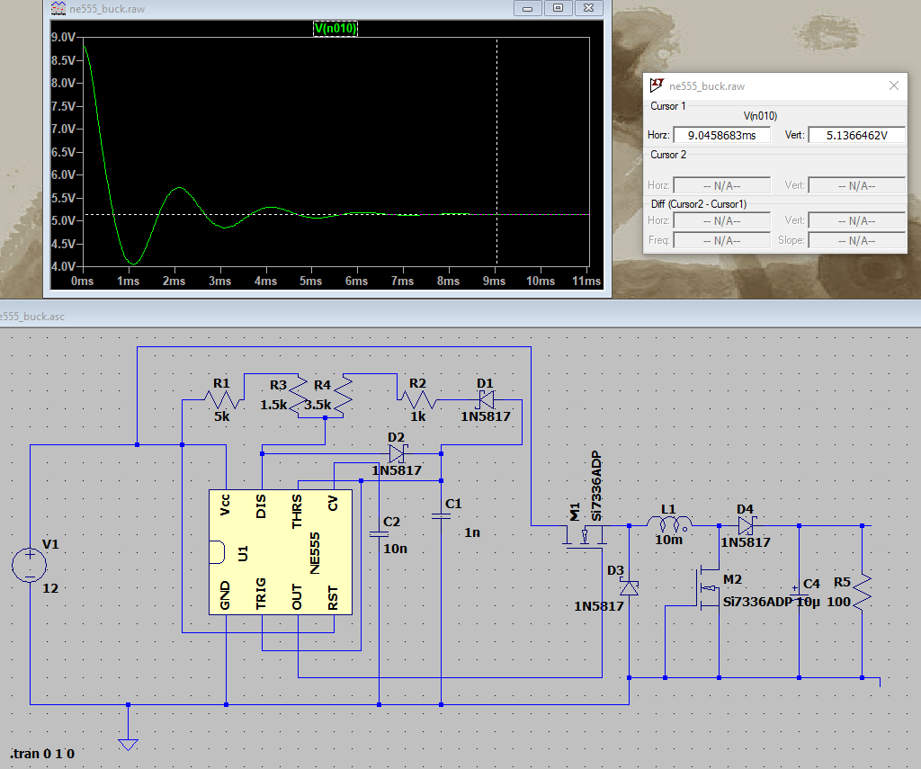
Day 2: Simulation or how is this even supposed to work?
12/14/2021 at 22:03 • 0 commentsMy first attempt at solving the problem is going to be throwing some simulation at it. I’m not so sure about buck converter, so I’ll start with that. Essentially, it can be split into a square wave generator and a buck converter stage. From there, it should be possible to derive correlation between duty cycle and the output voltage and final problem will probably be how to control one with the other.
LT spice adventure
Although I’v never used LT spice for simulation, it isn’t that bad and things make sense for the most part, but where is your potentiometer, LT spice?
My initial idea on NE555 in configuration that allows the frequency to be kept more or less constant, while the duty cycle can be adjusted by controlling R3/R4 to tweak charge discharge path of the capacitor C1. Something like this:
![]()
After some tweaking of R3/R4, it seems like 1.5k/3.5k (5k potentiometer) works for input voltage of 12V. Following some initial settling time, voltage remains on 5.1V, So first piece is done, we have a buck converter that takes 12V and spits out strong 5V :D
The output voltage, however depends on input voltage so for a range of input voltages, there needs to be some feedback that adjusts the PWM. This has to do with energy deliver into to buck stage of the converter per single pulse of the generator. So next step here is going to be figuring out a way of closing the loop and bring feedback from buck stage into the PWM generator...
-
Day 1: Requirements (what are we doing?)
12/13/2021 at 19:22 • 0 commentsServo motors feature a standard 3 pin connector that most often requires GND, 5V and 'signal'; in that order. So to make things convenient, tester needs to feature a single 3-pin output that matches.
One of the pins is power output, which often implies there's a power input, too. Servos aren't too picky about their input but ~5V seems to be the safe area for keeping the magic smoke from appearing.
And finally, there's the signal output. Consulting the datasheet for a Futaba S3003 servo motor, signal is described as the pulse of a certain width at around 50Hz (20ms). By varying the pulse width, between 1 and 2ms (or 2.5% and 5% duty cycle) the position of the shaft changes between roughly -90 and 90 deg.
So the above can be summarized to a couple of bullet points:
- 3-pin output (GND, 5V and 'signal')
- 2 pin input (some kind of voltage, higher or equal to 5V)
- Buck converter to drop voltage higher than 6(ish?) volts to 5
- PWM generator fixed to 50Hz, with 1.5 +/-0.5ms pulse width
Stretch goal:
- both buck/boost in one to support a wider range of input voltages
"Now hold on, what's the big deal here?" you might ask, "PWM generator with NE555 is nothing special and buck/boost module can be bought online relatively cheap".
Well, the idea is to to build everything up from scratch using NE555 in both the PWM stage, but also a buck(/boost) converter as the driver ^^ Then we can hopefully qualify to the 555 Timer contest. NE555 is truly an awesome little chip! It happens to be the first IC I touched when starting up with electronics and so I thought it would be fun to revisit the basics again...