 Mario Ninic
Major requirements for this probe project:
Bandwidth: up to 20MHz
Attenuation: x100, x10
Maximum input voltage: up to 500V differential
Differential Input Impedance: 8MOhm || 10pF
Power supply: External 5Vdc
Note:
Since this probe is for my own use, I did not incorporate any protection devices such as MOV, clamping diodes or fuse. If you decide to build device similar to this, please familiarize yourself with the danger related to usage of this probe.
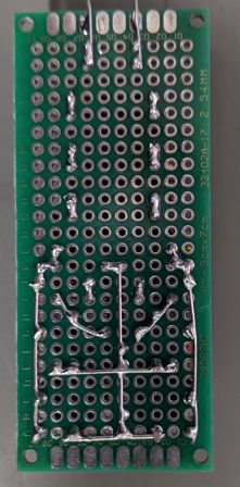
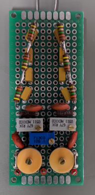
Construction details
I designed input attenuation circuit first starting with my requirement for attenuation factor of 100 and input impedance of 8 MOhm. Since differential circuit is symmetric, I designed one half circuit with 4 MOhm and 1:100 ratio. The combination of resistors that fits this ratio is 3.96M and 40k.
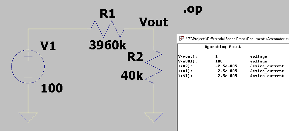
I had some 1.3 M resistors 5%, 25ppm temperature coefficient and I hand selected values closest to the 1.3M. Three of them should be close to 3.96M. For the 40k resistor I choose 39k and 1k trim pot for adjustment. I should use 0.1% tolerance resistors but I wanted to reuse as many parts as possible.
The compensation capacitor was chosen next as per requirements, 10pF or less for the differential configuration. Again, I use what is on hand, 47pF / 200V capacitors. 4 of them in series per R1 leg. This will equal to 11.75pF +/- 10%. Differentially it equates to around 6pF plus stray capacitance. which is confirmed by rough, in circuit measurement. The serial combination of 4 capacitor with 200V each will add up to 800V per leg.
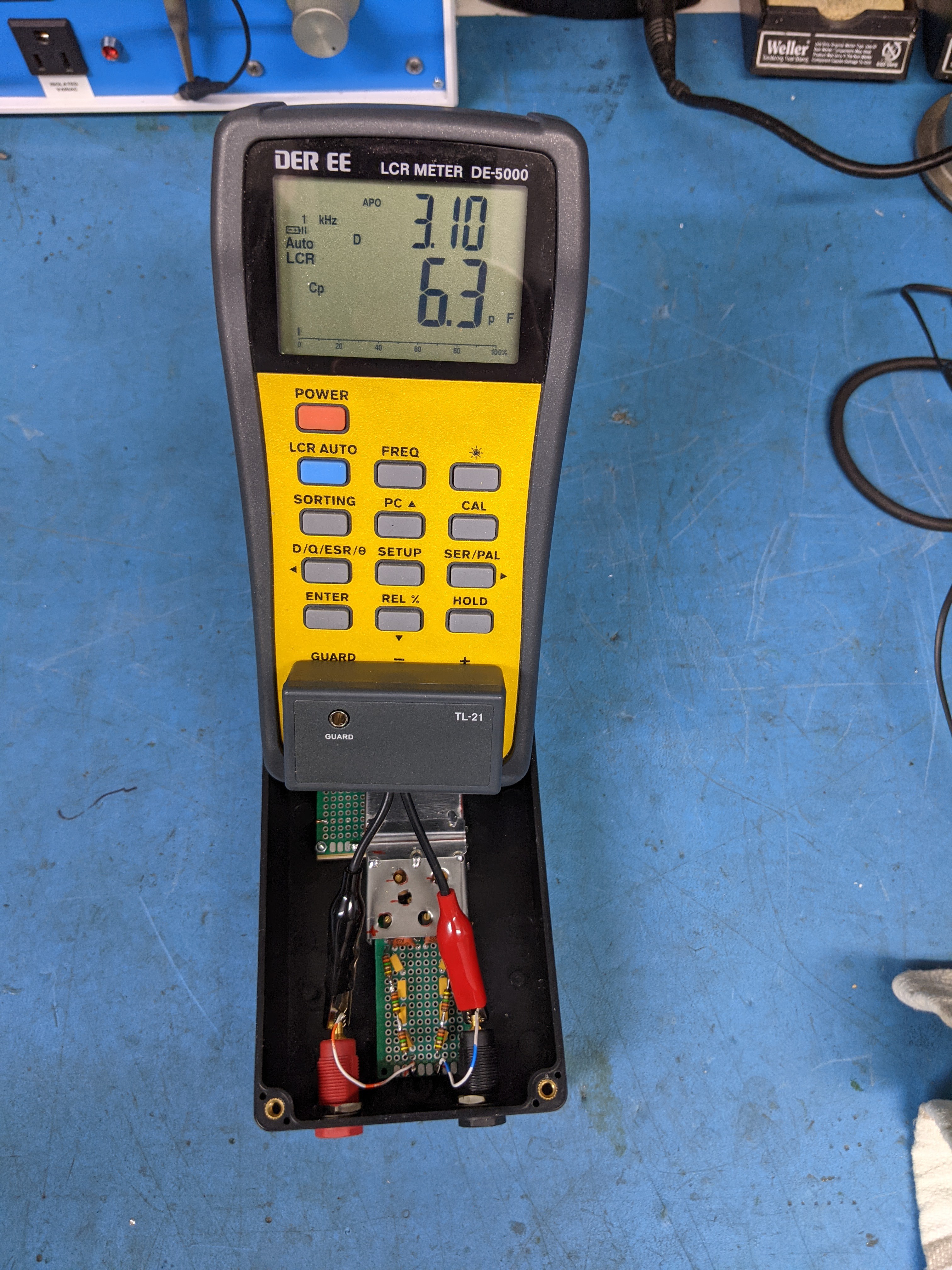
The second compensation capacitor is chosen to have same ratio as voltage divider. I chose 960pF in parallel to trim capacitor 25 to 180pF which will give the required adjustment ratio of 985pF to 1140pF.
Constructed attenuator looks like this:
At this point the attenuator circuit could be tested and adjusted if needed. I used 30V power supply to verify and adjust 0.3V at the output.
The x10 range is obtain by amplifying x100 range by factor of 10. The best opamp I have on hand was AD8066, fast FET with 145 MHz bandwidth. The differential to single ended configuration or instrumentation amplifier is standard from the datasheet and it is used in many of the low speed probe design.
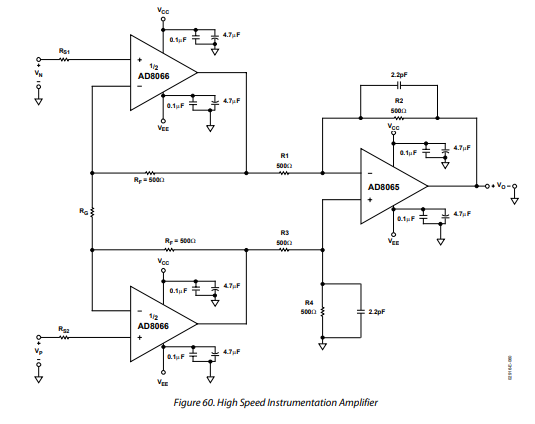
Schematic taken from the AD8066 datasheet from the www.analog.com
The value of gain resistor is calculated using following equation:
Vout = (Vn - Vp)*(1+2R/Rg)
Where R assume all resistors are the same (in my case 1kOhm) Solving for Rg I get Rg=222.22 Ohm for gain of 10.
Completed schematic is shown below.
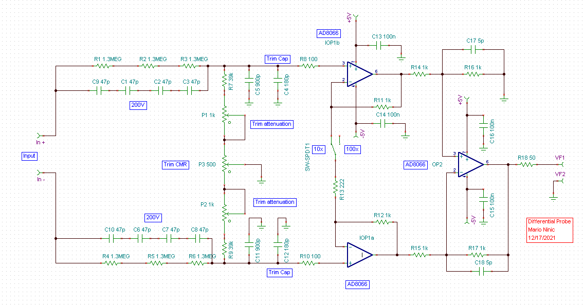
For the power supply circuit I used Murata NMV0512SC dual output DC-DC converter in conjunction with the LM7805 and LM7905 to get down to +/-5V. It was not optimal solution but 7V drop across the regulator was tolerable since opamps current draw was minimal. The 5V power supply's from the old cellphones are plentiful.
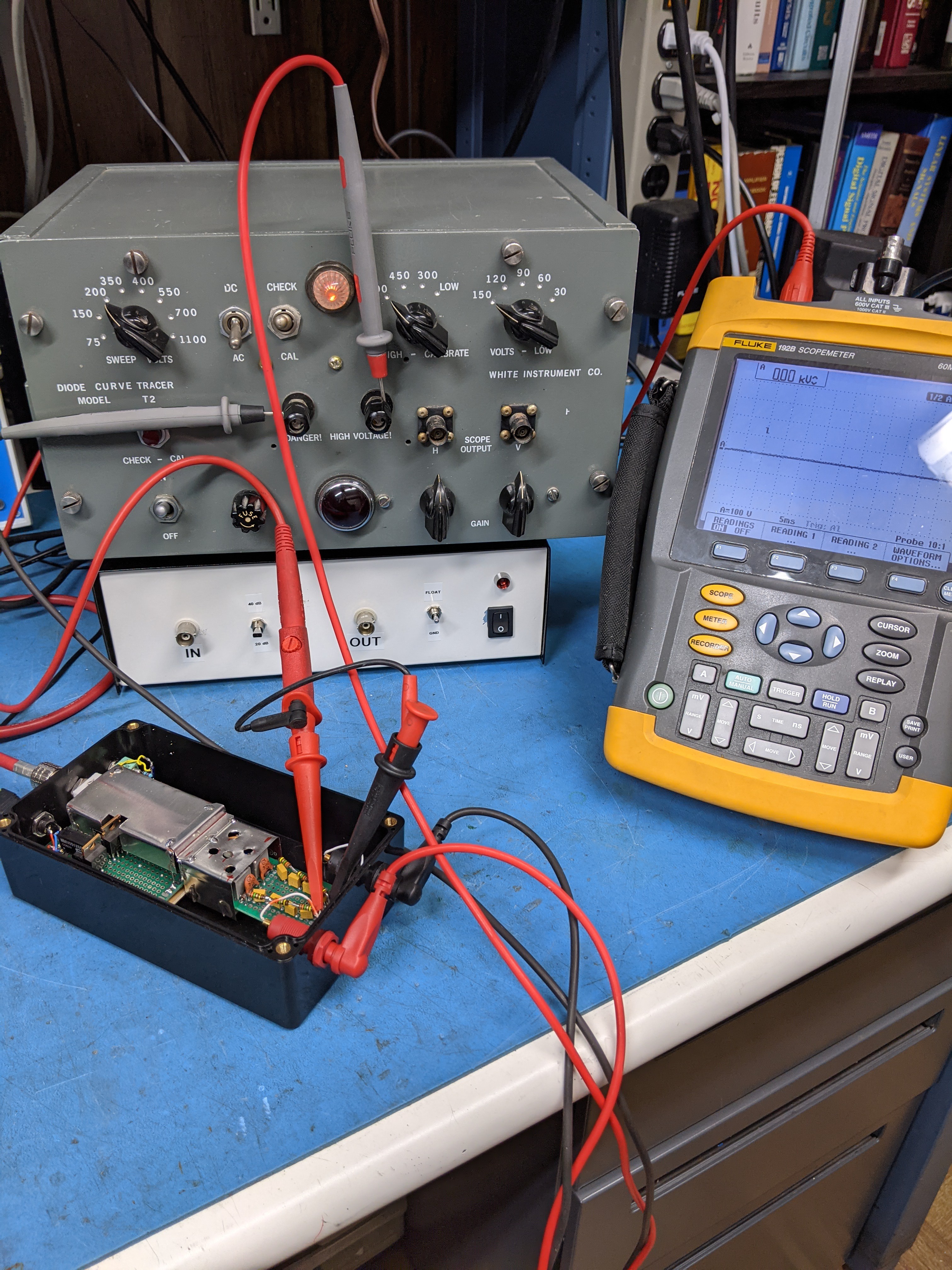
Test results.
Test setup:
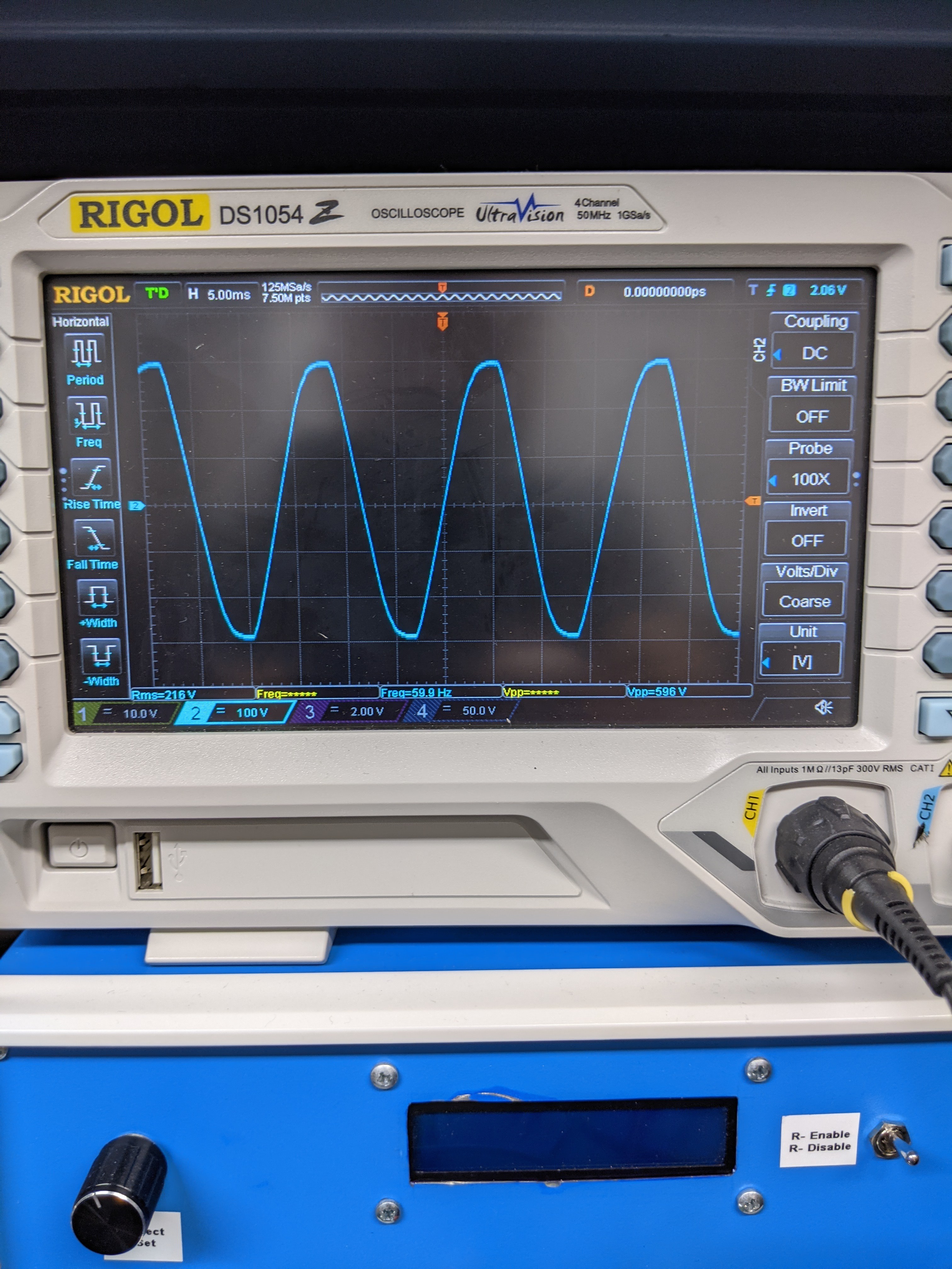
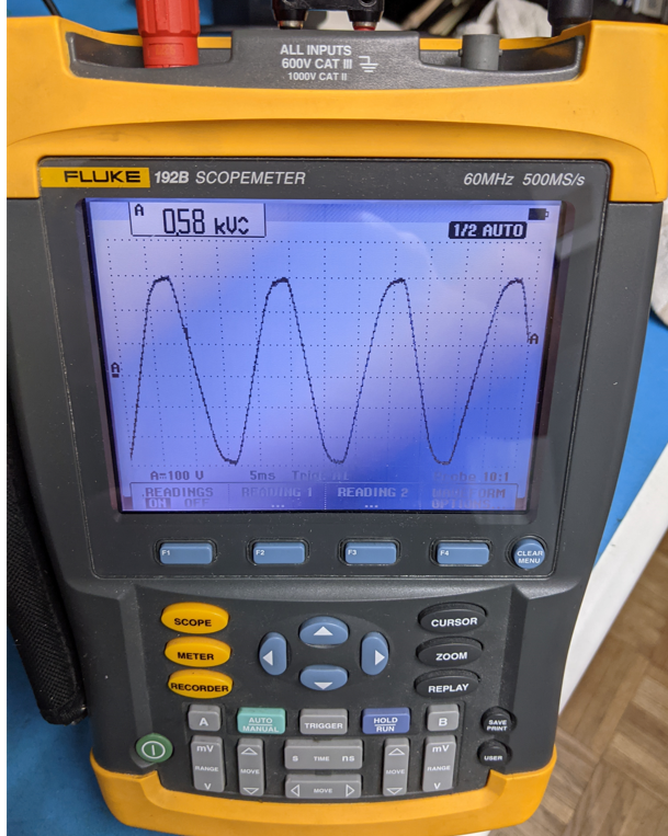
Correct measurement for the 200Vrms.
 hesam.moshiri
 Lithium ION
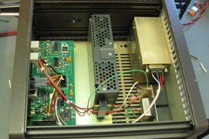
 Quinn
Quinn