Close
0%
0%

MCU-Less DS1302 Calendar Clock

Doing SPI with a microcontroller is boring. Why not do it with dozens of logic chips and 555 instead?

Similar projects worth following
A DS1302 calendar clock that is controlled via SPI with 30+ logic chips and 555 timers. The circuit can read and write time registers from the RTC and output them as a set of 8-bit BCD parallel output. The design is also modular and allows multiple types of output boards to be connected such as 7-segment or nixie tubes.

The project is currently in progress:
[DONE] Time register read circuit
[DONE] Parallel output stage
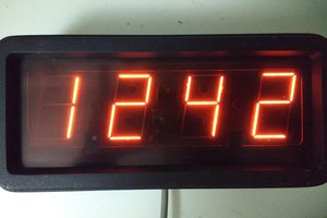
[DONE] 7-Segment output board
[DONE] HV boost converter circuit for nixies
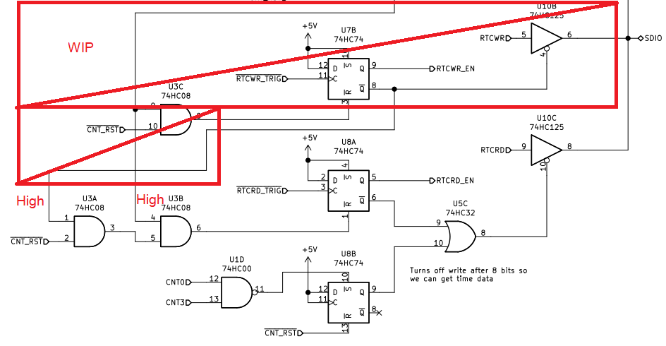
[Debugging] Time register write circuit
[Debugging] Write-Protect (WP) bit clear circuit
[Debugging] SPI bus arbitration circuit
[Planned] Display dimming circuit
[Planned] Nixie output board

Note: The component list on the project page only lists the chips I use. For the full parts list, please check out the attached KiCad files. 

-------------------------------------

This clock is my third clock. The first two (TTL clock and Ammeter clock) are nice and work fine. However, there is one common problem: 

I have to set the time again if I unplug it. 

This starts to get very tedious. Especially during debugging that I have to unplug it often to fix stuff, or to change where I place my clock, or when there is a blackout, so I know that on this one the time must be battery-backed.

Therefore this clock was born. It uses a DS1302 battery-backed SPI RTC chip to store and count the time. A 555 timer controls the sampling of time from the RTC 10 times a second with an SPI transaction at the speed of around 150 kHz (from a second 555 timer). The time read will be dumped onto a set of shift registers, which could be used to drive all kinds of displays from 7-segment to nixie tubes.

The clock also includes a circuit to allow the user to clear the write-protect bit and set the RTC time via DIP switches. The priority-based bus arbitration circuit allows the SPI transaction to complete smoothly. (This part is still under development.)

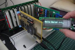
Currently, I built a 7-segment output board for the clock. The output board features 6 sets of 7-segment displays that are used to output year, month, date, hour, min, and sec, and a linear display to show day-of-week. A 555 timer and several logic chips are used to control display multiplexing.

The project is still under development. If you have any suggestions apart from the ones listed above. Please feel free to leave a comment. Thanks for reading!

mculess_ds1302_segment_output_sch.pdf

Main clock circuit schematics

Adobe Portable Document Format - 132.82 kB - 01/02/2022 at 19:36

Preview
Download

mculess_ds1302_sch.pdf

7-segment output circuit schematics

Adobe Portable Document Format - 271.94 kB - 01/02/2022 at 19:35

Preview
Download

mculess_ds1302.zip

Main clock circuit KiCad project

x-zip-compressed - 1.07 MB - 01/02/2022 at 19:35

Download

mculess_ds1302_segment_output.zip

7-segment output circuit KiCad project

x-zip-compressed - 141.72 kB - 01/02/2022 at 19:35

Download

  • 2 × NE555 Discrete Semiconductors / Power Transistors and MOSFETs
  • 1 × 74HC00 Electronic Components / Misc. Electronic Components
  • 2 × 74HC08 Electronic Components / Misc. Electronic Components
  • 1 × 74HC14 Electronic Components / Misc. Electronic Components
  • 1 × 74HC32 Electronic Components / Misc. Electronic Components

View all 18 components

  • Output - 7 Segment Board

    Sleepy Pony01/06/2022 at 17:48 0 comments

    This is a short log about the 7-segment output board. It consists of 12 7-segment digits grouped into groups of two digits for displaying year/month/date/hour/min/sec and a set of 7 discrete LEDs for displaying day-of-week (one LED for each day).

    At first, I think I will need to drive each segment separately, but that means 12 driver chips and 7 resistors for every digit. This would be a nightmare to assemble (too many parts and connecting wires). Fortunately, after fiddling with the 74HC595 output stage I found a solution that will let us multiplex these displays!


    The segments

    The 7-segment displays part is wired in a pretty basic multiplexing configuration: cathodes connect together and anodes are used to control which set of segments to enable at a time via a PNP transistor. You can see that for each group of 7-segment, I control both anodes at the same time and cathodes are separate into groups of tens digit and ones digit. This will make more sense later.

    7-Segment Displays
    7-Segment Displays

    Days-Of-Week Display

    It would be silly to put days-of-week on a 7-segment display showing numbers 1-7 because that's boring. Here I choose the 74LS138 chip to drive 7 LEDs which indicates Monday to Sunday. I wired the 3-bit input of 74LS138 to the lowest 3 bits of the data input because the register that stores DoW could only have values between 1-7 (001 - 111, 3 bits), and also wired the LEDs to output pin 1-7 accordingly. Note that the output is active low so the chip should be used to sink current.

    Days-Of-Week Display
    Days-Of-Week Display

    The Data Inputs

    You might remember from the last log that out clock output data of the 7 date-time registers parallelly through 7 sets of 8-pin headers. However, the neat tricks I will talk about later allow us to just tie all of these headers together and select which register would be outputting the data.

    Here you can see that we have a pair of classic 74LS47 BCD to 7-segment decoder chips for tens and ones digits. Since DS1302 output data is in BCD format we can directly use the upper 4 bits for tens digit and the lower 4 bits for ones digit.

    Inputs are all tied together!
    Inputs are all tied together!

    Where The Magic Happens

    From the last log, you can see that all of the 74HC595 output stage registers have their Output Enable (~OE) pins pulled down and connected to an 8-pin header to the display.

    By default, all of the registers will output their data all at once. But if we could drive these ~OE pins all high but one, we can choose which register outputs the data.

    Shift Register Output Stage, From the Last Log
    Shift Register Output Stage, From the Last Log

    This part of the circuit on the display controls this behavior. First a 555 in astable mode provides a display scan clock at around 380 Hz. This clock is used to drive a CD4516 counter, which in turn connects to a 74LS138 Decoder. This chip will output high on all outputs except the one matching the binary input value (for example, if you input number 3 output O3 will be low while all others are high). 

    Sounds familiar? Yes, if we connect this to the registers ~OE pins and segments anode control pins (or ~EN2 pin of the Days-Of-Week decoder chip) we could scan the entire display!

    The Output Selector Circuit
    The Output Selector Circuit

    The result turns out to be pretty great. There is no difference between using 12 chips to drive 12 segments and multiplexing them. Here we use only 6 chips instead of 12, and we saved a lot of headaches.


    And here's how the display works! Thanks for reading!

  • Control Circuit - Reading The Time (Part 2)

    Sleepy Pony01/05/2022 at 15:51 0 comments

    Continues from Part 1


    Chip Enable

    To communicate with DS1302, we need to hold the Chip Enable (CE) signal high throughout the transaction and return it to low after the transaction ends. So in this part of the circuit, I OR the enable signal from all three types of the signal together to enable the SCLK and CE signals.

    Note: This circuit is part of the SPI bus arbitration circuit which is not in full working order yet at this point of writing, so pin 13 of U3 is force high for the time reading part to work.

    CE Signal Control
    CE Signal Control

    Time Burst Read Command

    We need someplace to store our time burst read command (0xBF). In this case, I choose a 74HC165 Parallel-to-Serial Shift Register for this job. By being a shift register it works like a typical SPI bus, and by having a parallel-load feature we could set the value we need as a parallel input and load it into the register each time we start the transaction. Perfect.

    Time Read Command Store
    Time Read Command Store

    In Or Out?

    SPI is actually an easy protocol to make a logic circuit for. You generally just need a clock source and two sets of shift registers connecting in a circle. However, DS1302 complicates that by sharing MOSI and MISO pins. This forces us to control the data direction in and out of the chip according to the number of clock pulses that already passed: output for 8 pulses and then input for 64 pulses.

    Luckily, the step counter CD4040 we use to count 72 pulses of SCLK breaks out every counting bit out, so we can tap the counter at the 9th pulse to switch the data direction.

    To switch the direction, we will use a 74HC125 Tri-State Buffer. This kind of buffer is convenient when we need to isolate one part of the bus from another just by disabling the buffer. Here, we use it to isolate the command store register from the SDIO pin after 8 bits of command were sent.

    Note: This circuit is part of the SPI bus arbitration circuit which is not in full working order yet at this point of writing, so pin 1 and 4 of U3 are force high for the time reading part to work.

    To summarize this part of the circuit which is probably the most confusing part, first, the ~RTCRD_TRIG signal from the time read timer will cause the command store U24 to load 0xBF into the register on the falling edge, then on the rising edge, U8A will latch high, causing the RTCRD_EN signal to go high which in turn causing the CE signal to go high and also enable the SCLK clock. 

    At this time U5C will output low, enabling the tri-state buffer U10C which will allow 0xBF to pass to the SDIO pin. At the 9th rising edge of SCLK however, CNT0 and CNT3 signals will both go high (2^0 + 2^3 = 9) and set the U8B flip-flop to high. This will disable the U10C buffer to allow DS1302 to output data onto the bus. SCLK will continue for 64 more cycles before the ~CNT_RST signal goes low and reset everything back into the initial state.


    Storing the Output

    DS1302 should output the date-time data on the bus at this point. We will need 8 bytes of storage to store the data before we could output it to the display. I choose to use 8 of 74HC595 8-Bit Shift Register with Tri-State Output Registers. There are many aspects of this popular chip that makes it perfect for our use case.

    • The outputs are Tri-State, which means we could choose to enable one specific chip to output at a time, making multiplexing the output at the display easy.
    • The outputs are also buffered. We can freely shift the data into the chips and then latch the data to the output when we are ready. The shifting action will not be seen on the outputs.
    • The chip can be chained together, and all output bits are available for use.

    Here you can see the registers are chained together into a big 64-bit register. The data input pin SER is connected to the SDIO signal. Shift clock SRCLK is connected to SCLK, and output latch clock is connected to RCLK signal, which is actually CNT_RST signal i.e. that data will be outputted when the 72nd clock pulse was reached....

    Read more »

  • Control Circuit - Reading The Time (Part 1)

    Sleepy Pony01/04/2022 at 16:40 0 comments

    POR Reset: Getting Everything In Sync

    Before we get into the logic of reading the time out, there is another thing we have to take care of first: We have to make sure that the circuit is in the correct state every time it powers up. This is called a Power-On Reset (POR) circuit.

    We can build it simply with an RC timing circuit and a couple of transistors. When power is connected, the reset signal is in one state (reset), then the capacitor will be charged up at a specific rate and then turns the transistor on or off, locking the reset state in another state (run) forever.

    Simple POR circuit from another project
    Simple POR circuit from another project

    However, in this project, I've decided to use a dedicated chip for the purpose: TL7705A

    The TL7705A is a supply-voltage supervisor for 5V systems. To put it simply, this chip will hold a circuit it is supervising in a reset state (both active low and high outputs are available, very convenient) until the supply voltage reaches a specific value (3.6V in this case) then it will release the reset signal and let the circuit runs. It only requires a single capacitor to set the timing. I use the circuit below to generate a 1.3ms long reset pulse.

    Datasheet here: https://www.ti.com/lit/ds/symlink/tl7705a.pdf

    TL7705A POR Circuit
    TL7705A POR Circuit

    The Reading Steps

    From what we know about DS1302 in the last log, we see that we need to follow these steps to get the date-time data out.

    1. Get our SPI bus into write mode.
    2. Start the SPI transaction by driving the CE signal high.
    3. Enable the SPI clock, then send the clock burst command 0xBF to the RTC.
    4. Switch the SPI bus into read mode.
    5. Send 64 additional clock pulses to get 8 bytes of date-time data (including WP byte) out, and then store it somewhere. (Noted that we need to send out 72 clock pulses in total.)
    6. Stop the SPI transaction by driving the CE signal low.

    The Clocks (pun intended)

    We need two clocks in the system, one to trigger time reading and another to act as an SPI clock. 

    The first clock is easy. A rather slow 555 Astable circuit will work just fine. I decided to use 10 Hz.

    Time Read Trigger Clock
    Time Read Trigger Clock

    The SPI clock could be made much faster because DS1302 could work up to 2 MHz but there's no need to push that limit. I use only 100 kHz. Again this is also a 555 Astable circuit, but with some twists.

    SPI Clock
    SPI Clock

    You can see that the reset pin is connected to SCLK_EN signal. This signal is high when something needs an SPI clock. By connecting it to the reset pin it ensures that we get full clock cycles right from the start every time. Without this, I observed that the display often glitches out because the first clock pulse is too short (i.e. we enable the clock in the middle or at the end of the 555 cycles).

    Another point is that we have both SCLK and ~SCLK signals outputs. From the DS1302 datasheet, we can see that we need to put the data on the bus on the falling edge and the chip will sample data/put data on the rising edge. Therefore we need to put the DS1302 and the receive circuit on the SCLK signal and put the transmit circuit on the ~SCLK signal to make everything in sync.


    Counting the Pulses

    To read the time correctly, we need exactly 72 SPI clock pulses (8 for command byte, and 64 for 8 data bytes). More or less than 72 pulses will result in a display glitch. Here I use a 12-bit counter to count the SPI clock and send a reset signal out when it reaches 72 (2^3 + 2^6 = 72). This is a common trick to reset the ripple counter prematurely.

    SPI Clock Counting Circuit
    SPI Clock Counting Circuit

    [This log will continue in part 2.]

  • DS1302 - How We Keep Time

    Sleepy Pony01/03/2022 at 16:17 0 comments

    What is an RTC?

    The heart of this clock is a battery-backed RTC chip. Real-Time Clock (RTC) is a type of interface chip that is responsible for the timekeeping of the system. An RTC with a battery-backed feature means the chip has a separate power source for the chip to keep the time when the main power fails, which means I don't have to set the time again every time I unplug it.


    DS1302 Trickle-Charge Timekeeping Chip

    There are many choices of RTC chips available on the market today, I have decided to use DS1302 for many reasons:

    • A cheap, well-known chip that is widely available.
    • Uses SPI protocol to communicate which is very easy to control with logic chips. (More on this later.)
    • Has all of the timekeeping features I need: Year/Month/Day/Date/Hour/Min/Sec.
    • Data output is in a BCD format, which is ideal for a 7-segment decoder chip.
    • Has a burst I/O feature. (More on this later.)
    • Available in DIP package.
    • Has a battery-backed feature. This chip could also trickle-charge a rechargeable battery by itself (but I use a single-use battery so I leave it disabled).

    Datasheet is here: https://datasheets.maximintegrated.com/en/ds/DS1302.pdf


    How should we make it tick?

    DS1302 Block Diagram
    DS1302 Block Diagram (from datasheet)

    First is the block diagram. We can see that we need to:

    • Connect the main power source to VCC2 pin.
    • Connect the secondary power (backup battery) to VCC1 pin.
    • Connect the ground pin (obviously).
    • Connect a quartz crystal between the X1 and X2 pins. Noted that from the datasheet we will know that we need a 32.768 kHz crystal with a 6 pF load capacitance value.
    • Connect the SPI bus to the remaining 3 pins. Noted that this chip shares the SPI MOSI and MISO pins. This will be very important later.

    So now we have this circuit below:

    Note: I do include 100nF decoupling capacitors at every Vcc pin on every chip, but I put these all in the power input sheet, so they will not show on the pictures.

    DS1302 Circuit
    DS1302 Circuit

    Communications

    DS1302 SPI Communication
    DS1302 SPI Communication (from datasheet)
    DS1302 Commands List
    DS1302 Commands List (from datasheet)

    Communications with the chip use a common SPI protocol. First, we drive the chip enable (CE) high, then we feed our clock signal in the SCLK pin, and read/write the data on the I/O pin. However, from the datasheet there are some important points:

    • The first byte we send to DS1302 is a command byte, which tells which register and region to read/write from and if this command is a read or write command.
    • DS1302 will switch from read to write mode automatically after 8 clock pulses if the command we send is a read command.
    • The data going in/out of the chip is LSB-first.
    • The data stored on the chip are organized into a set of 8-bit registers. We can read or write a specific register, or we can access full date-time data in one go by issuing a clock burst command.
    • clock burst command, when issues on the clock bank, will output full 8 bytes of time data and 1 extra byte that contains a write protect (WP) bit indicating if we could write to the chip or not. 
    • We need to clear the WP bit by writing 0x00 to 0x8E register before we could write anything to the chip.

    From what we gathered from the datasheet, to build an MCU-Less clock based on this chip we would need to have the following:

    • An SPI clock source
    • A sampling clock source (to query time from the chip)
    • A CE signal controller
    • An SPI bus I/O direction controller
    • An SPI bus arbitration controller (to make sure commands are executed in a correct priority and did not interfere with other commands)
    • A place to store DS1302 clock burst read (0xBF), clock burst write (0xBE), and WP write (0x8E) command bytes
    • A place to store time data we got from the chip
    • A place for the user to input new time data (plus related control logic)
    • A place for the user to clear WP bit
    • A way to make sure everything starts up correctly when powered-up (POR reset)
    • A display that will show the date-time data
    • A power source
    • And other misc logic features

    You can see there's quite...

    Read more »

View all 4 project logs

Enjoy this project?

Share

Discussions

Similar Projects

Does this project spark your interest?

Become a member to follow this project and never miss any updates