 Dave Collins
Introduction and explanation:
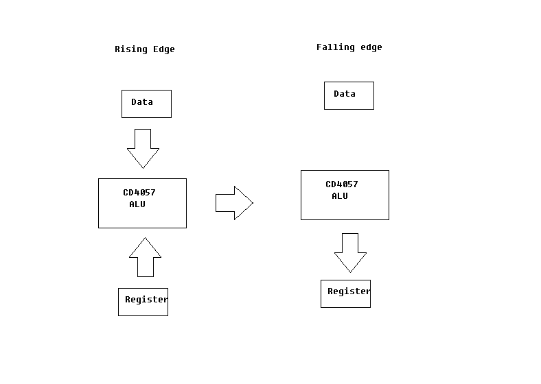
In the current project version of the clock module I wanted to have a clock module that had a fairly stable state, that had clean /CLK and CLK transitions (with no delay between the inverse and non-inverse state of the clock) both heaving a 50% duty cycle. Also, I needed to be able to half step through a clock cycle in order to see the data states at the high to low (and low to high transition). The main reason for this is the accumulator register is compared with the data bus on the rising edge in the ALU and clocked into the accumulator latch on the falling edge ( replacing the previous value from the latch, which was used by the ALU during the rising edge. )
These transitions ideally will happen thousands or even millions of times in a second, and so it's important to have a clock that can properly supply carefully timed rising edges where we need them in order to facilitate these calculations without running into trouble. If we use a simple inverter on the clock from a 555 timer, when we being to run tests at faster speeds the propagation delay becomes significant. The solution is simple, generate both clock pulses simultaneously and eliminate the delay. We can do this many ways, using two parallel XOR gates, buffering the clock with similar parts , or as I've done use a clock divider and only focus on the rising edge of the clock. By latching the clock with a D-Latch, we assure a 50% cycle by only worrying about 1 thing, the rising edge of the incoming clock pulse.
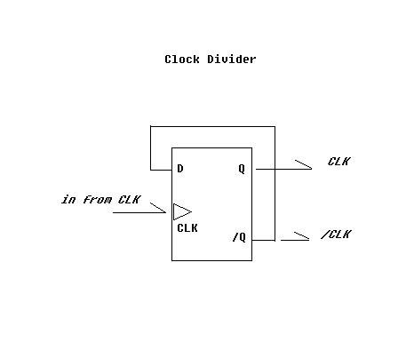
The incoming clock pulse can be at any duty cycle, and the resulting output will be based on the rising edge of the incoming clock pulse only. This has the advantage of generating a output that is exactly 50% of a duty cycle based on that rising edge, likewise the rising edge of /CLK is exactly at the same time as the falling edge of CLK. This has the glaring issue of reducing the incoming result from the oscillator by half, we can overcome this issue by building an oscillator that is twice as fast as we need.
R-C inverter Circuit
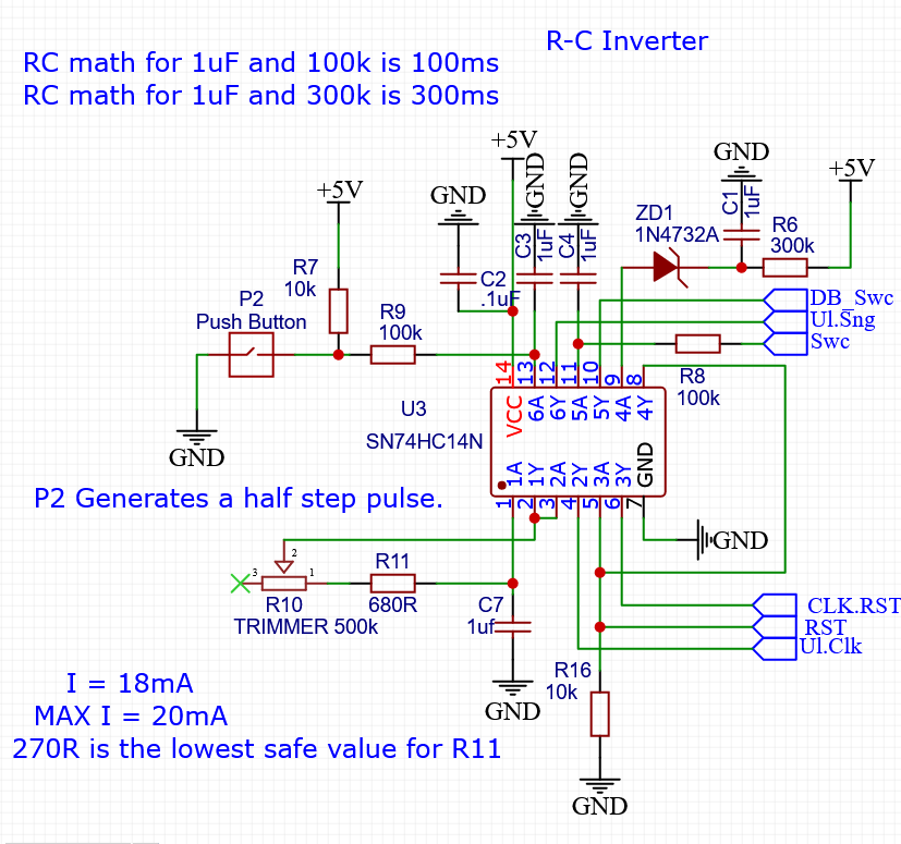 The resistor R11, and Trimmer R10 (combined with C7) provide the R-C network that makes up the main oscillator, as you can see this is essentially two Schmidt Trigger inverters tied together, the first with the resistors connected in feedback to create a very simple square wave oscillator. As I've discussed in previous Logs, this is a very common configuration for building an internal oscillator in a MCU, and has the benefit of being very "Parts Light". The reaming nets on the chip are used for generating Power On Reset (C1, R6 and ZD1), half step pulse (technically a single pulse generated by R9 and C3), and a de-bounced switch for the function select latch (C4 and R8).
The power on reset signal, is simply a R-C circuit with a ziener diode that assures the signal is not sent to the inverter until it is at least 4.7v (de-triggering the input to a much higher threshold.) This has the added benefit of dropping the CPU into a continual reset state if the V+ rail drops below 4.7v in the case of a near over current situation.
Function Select Buffer
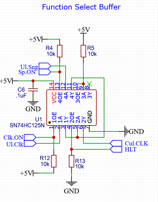
The function select is simply a Quad buffer package, the signals Clk.ON and Sp.ON are generated elsewhere (using a latch). The buffer holds both the Unlatched clock signal, and the single pulse clock in High-Z, using the pull up resistors at pins 1 and 13. We tie these signals low using a d-latch and it's Q and /Q outputs. The cumulative clock (either the unlatched clock or the single pulse clock, depending on the function latch) is held in an enabled state by pin 4 through a pull down resistor, and can be tied high using a HIGH signal latched elsewhere in the computer (most likely the flags register).
Clock and Control Latch
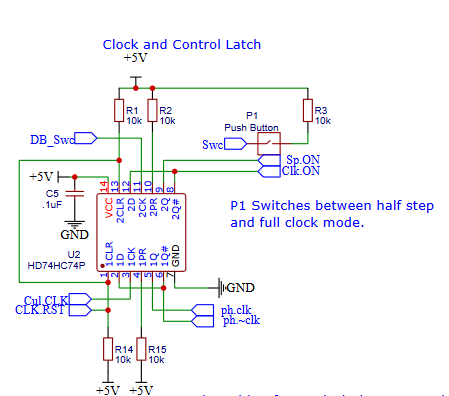
Latching the clock this way has all the above benefits of normalizing the clock, as well as saving the high sate of the clock through functional transitions and a halt. This is us full as we can see the state of all registers during a halt and a falling edge of a clock pulse generated by simply putting the clock into cut off won't cause unintentional errors.
Whats next?
I have plans to move on to building the accumulator for the ALU; this will be the first part of the build that uses a state machine to control the input to the 4 bit universal shift registers, these are needed vs a traditional d-latch as the ALU also supports a 1-bit rotate and shift operation. As always thank you for taking the time to look at my project, and feel free to ask any kind of questions that you might have in the comments. I hope everyone has a wonderful week, I'm finally feeling better and were on the trailing edge of the COVID infections that ran through our house over the last week, thankfully, the infections didn't turn out to be too bad or require any one of us to go to hospital, so for that I am very thankful.
Discussions
Become a Hackaday.io Member
Create an account to leave a comment. Already have an account? Log In.