 padnest
I designed the system memory mapping with these purposes in mind:
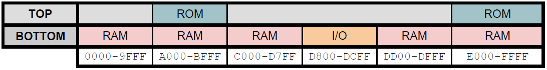
- to have 64Kb of RAM in the bottom layer
- to have 16Kb of ROM in the top layer
- to have the possibility of banking out the ROM having access to the background RAM
- any write operation on ROM is always addressed to the background RAM
- do not waste RAM mapping I/O devices
Memory layers:
Memory configurations
Bus lines EROM1 and EROM2 are used to enable or disable ROM layers: disabling the ROM you can read from the background RAM.
These lines can be programmatically controlled by one of the VIAs port.
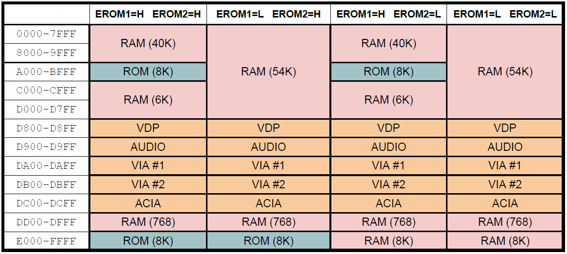
Each I/O device has 256 memory locations (one page) of space to map internal registers.
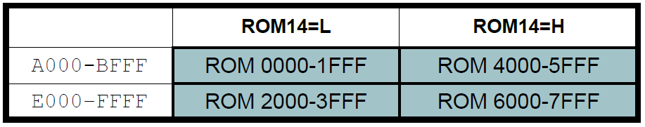
ROM banking
Since the ROM size is 32Kb we can have four 8Kb banks and so two different versions of ROM.
Bus line ROM14 is used to select which ROM locations are visible at the assigned ROM spaces.
Also ROM14 can be programmatically controlled by one of the VIA port (this might be a bit tricky to do at runtime!).
Glue logic
To implement all the chips selection logic just a single IC will be used: a programmable logic device (PLD).
This choise has many advantages (reduced number of components, easy to make changes, space optimization).
The PLD (an Atmel ATF22V10C) will be programmed following this table:
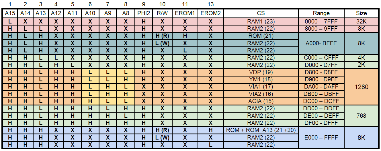
Inputs signals:
- A15 to A8: address lines
- PHI2: system clock used to match the RAM/ROM timings
- R/W: read/write line used to select background RAM on write
- EROM1, EROM2: ROM enabled lines
Output signals:
- 15 to 23: used to select the respective device (LOW level)
Next step: CPU board.
Ciao!
Discussions
Become a Hackaday.io Member
Create an account to leave a comment. Already have an account? Log In.