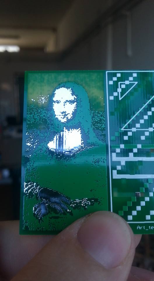
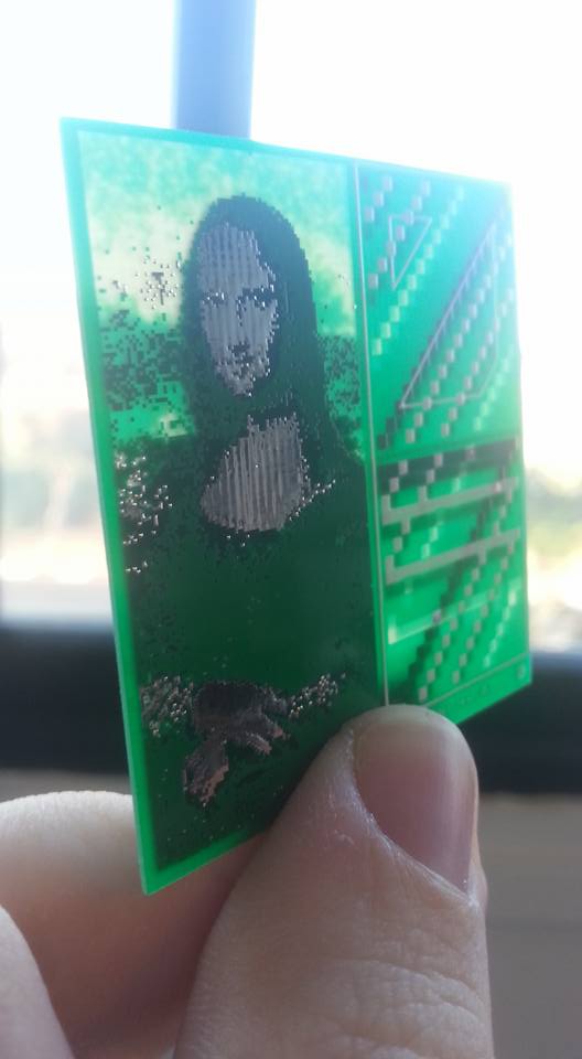
• PCB as an art medium

    alongruss11/20/2016 at 10:52 1 comment

    or: How I Learned to Stop Worrying and Love the Board

    Alon Gruss 20/11/16

    4.jpg5.jpg

    Tl;dr:

    I made a tool that converts an image into multiple PCB layers - pixel brightness to board opacity.

    source on Github

    1. You are not limited to your discipline!

    As a Designer by trade I like to jump head-first into new disciplines which I know nothing about, learn to control the terminology and try to mess around in unexpected ways. I am also lucky to share studio space with Arkadi Rafalovich, A talented engineer and omni-potentialite, who inspires and guides me through learning the basics of electronics and Eagle PCB design.

    While diving into the subject I was constantly visualizing and thinking about the tools that are missing for me, the tools I need for implementing my art and design.

    (I recommend Sparkfun’s tutorials).

    2. Most PCB’s are boring!

    PCB’s are usually designed functionally without any visual attention, A very boring rectangle. Sure, they have their digital charm with mazes of tracing running along the board, but as a user, I prefer my PCB’s when they're inside my products. Covered in a well designed injection-moulded shell.

    I use the word ‘usually’ because sometimes you get boards like the Defcon badge - which can masterfully merge function and design to create a fun user experience.

    Or this wonderful PCB-USB-Business card by Frank Zhao.

    3. The Artist in the Engineer

    So, what’s different in business cards and convention badges? These are where the engineer isn't working for a client, he relaxes a bit and has fun with the design tools. He’s not just a cog in the product development process. When he has no restrictions.

    Sadly, even then, the board designer dare only to use the tools given. Drawing only in the ‘Silk’/’Copper’ layers or slightly shaping the board’s outline in the ‘Dimension’ layer.

    4. All the layers!

    Some of my past Design projects deal with layered/laminated materials and the smart use of the different layer properties:

    IMG_20150511_072633.jpgגרוס_אלון.jpg

    Those were opaque materials. What intrigued me with PCB design-wise, was the ability to play with material’s opacity and the light transfer through the board. Artistically I thought I can convey a more complete message and user experience by having graphics that support and integrate with the board’s functionality.

    5. Testing the hypothesis

    I searched google for leonardo da vinci’s portrait of Mona Lisa (which I consider globally identifiable) and saved one of the results to my PC.

    Opened it up in Gimp. scaled it down (nearest neighbour) and duplicated it to a couple of layers.

    Mona_Lisa.png

    I then run a threshold filter on the layers changing the value a bit in each one and saved the layers to separate files.

    Only then have I noticed that the new versions of Eagle already have a built-in script for importing image, from colors to layers. “That’s great! This saves me a lot of time” or so I thought.

    Don’t misunderstand, It's a really great tool, just not for my purposes.

    You see, I need to control the cumulative combination of layer opacities in order to achieve my goal. I aim for the PCB to be facing up (showing the top layers).

    For example:

    • Lightest - clear from traces or solder mask on both sides.
      • ( no top + no bottom + yes tstop + yes bstop )
    • Light - clear from traces on both sides + solder mask only in back (bstop).
      • ( no top + no bottom + yes tstop + no bstop )
    • Medium - ...
    • Dark - ...
    • Darkest - ...

    We also have:

    • White Silkscreen - requires the top solder mask layer and the top silk layer
      • (... + no tstop + yes tsilk )
    • Copper trace - requires the top trace but without soldermask.

    You might have noticed that some layers control the lack of material and must be treated as a negative. That’s a bit confusing, so here is a guide table:

    ( legend: x = no || ⎷ = yes || ? = doesn't matter || n = inverted )

    Color

    (layer No.)

    Top

    (1)

    Bottom (16)

    tStop

    (29)

    bStop

    (23)

    tPlace

    (21)

    bPlace

    (22)

    0

    x

    x

    ⎷n

    ⎷n

    x

    x

    1

    x

    x

    x

    ⎷n

    x

    x

    2

    ?

    x

    ?

    x

    ?

    3

    x

    x

    x

    x

    x

    x

    4

    x

    x

    x

    x

    x

    5

    x

    x

    x

    x

    x

    6

    x

    ?

    x

    ?

    ?

    7

    ?

    ?

    x

    ?

    6. Lessons learned

    I ordered the boards from Seeed...

    Read more »