 Alexander Bissell
Material Selection:
I selected a 40mm silicon wafer to be the substrate for my first attempt as they are the cheapest of my collection and I have a bunch of them. For the photoresist layer I will be using the cheapest roll of dry film photoresist that amazon has to offer. [Note: turns out this was a really bad idea as this roll came with a ton of defects.]
After cutting a square of resist I removed one side of the film (a little piece of tape helps a lot here) and got to work trying to get it to lay flat on the wafer. This process is very similar to putting a screen protector on a phone, and seeing as how I have been doing that since the OG nintendo DS I thought I would have no problems.
This was a faulty assumption.
Laminating the wafer:
It turns out that getting that film down without any bubbles is very difficult. I tried plastic cards, blades, finger tips and vacuum chambers and still could not get all the air cleared out. Part of me wonders if I need to dehydrate the chips first? I'll try that next time for sure.
Once the film was on as flatly as I could get it, I set my trusty cricut heat press to 100c and set it on top of the resist+silicon for 2 minutes. This resulted in what appears to be pretty solid adhesion. I'll have to do some tests to see what affect this on the final outcome once I have the process down. I found it helpful to have a kimwipe underneath and on top of the stack to prevent the film from sticking to the press or the build plate.
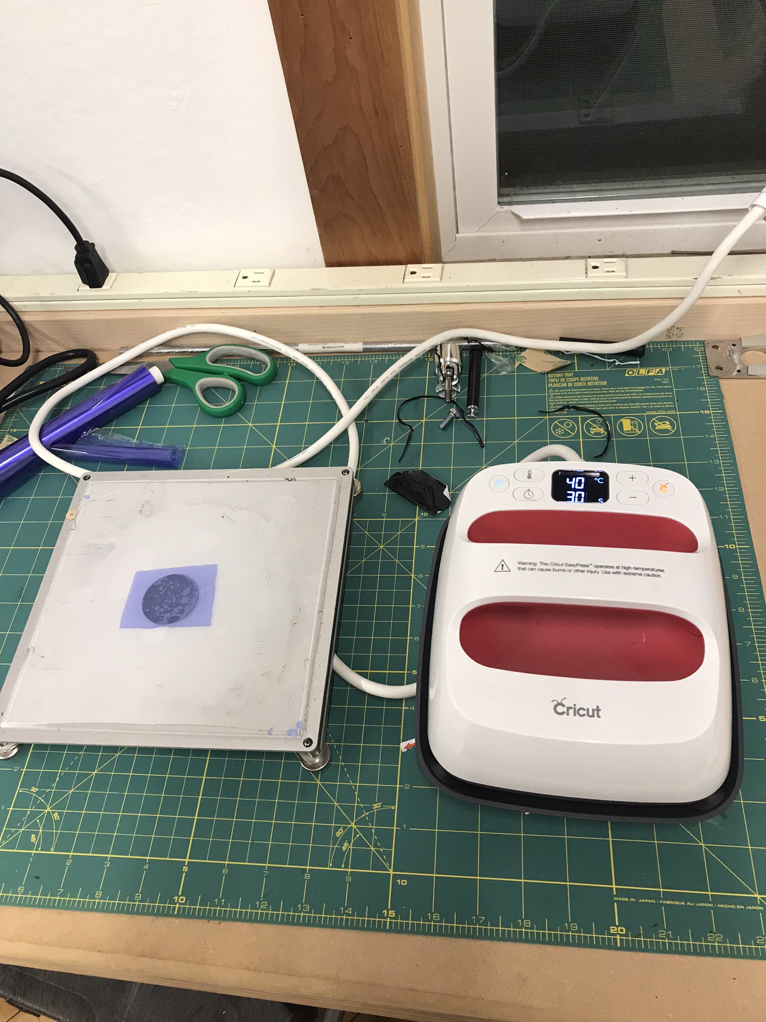
A quick word on the cricut easy press:
It's great. I got it for like $50 on sale at a Michaels and its been so useful for so many different projects. You program in the desired temperature, set a time, and you're good to go. It heats up quick and is really comfortable to use. The ceramic heating element is really flat and consistent too.
I fanboy over this thing so hard because I spent literal years looking for somewhat decent hot plates and heating presses and this thing blows them all out of the water. Cannot recommend enough.
Exposing the resist.
Dry film photoresist works by hardening when exposed to UV light. Usually a mask (can be from an inkjet printer, mylar, steel etc.) is placed on top of the resist and is then placed in a box with a UV light source. The UV light cures the photoresist in all the areas that the mask isn't covering which makes it resistant to the developing agent. This method works very well, but masks can be really expensive to produce and it is tough to make revisions once made. Inkjet printers work well enough for larger channel geometries, but we are trying to get below 100 microns wide here so "well enough" won't cut it.
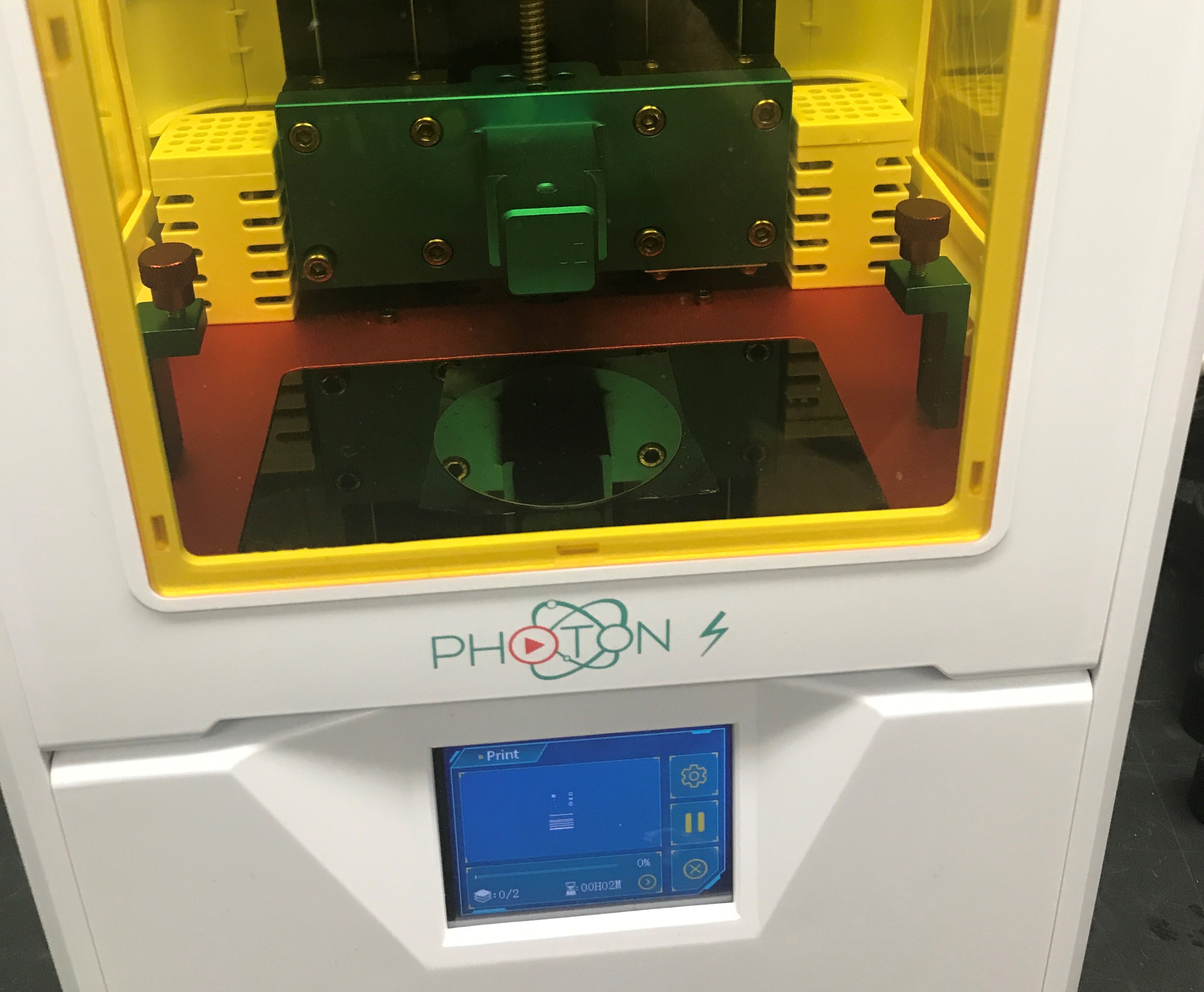
Enter the 3D resin printer.
A resin printer is basically just a vat of goop sitting on top of a small, high resolution monochrome UV LCD screen that displays an image and hardens the resin in that particular spot. Remove the vat of goop and it seems like a very good candidate for maskless photolithography.
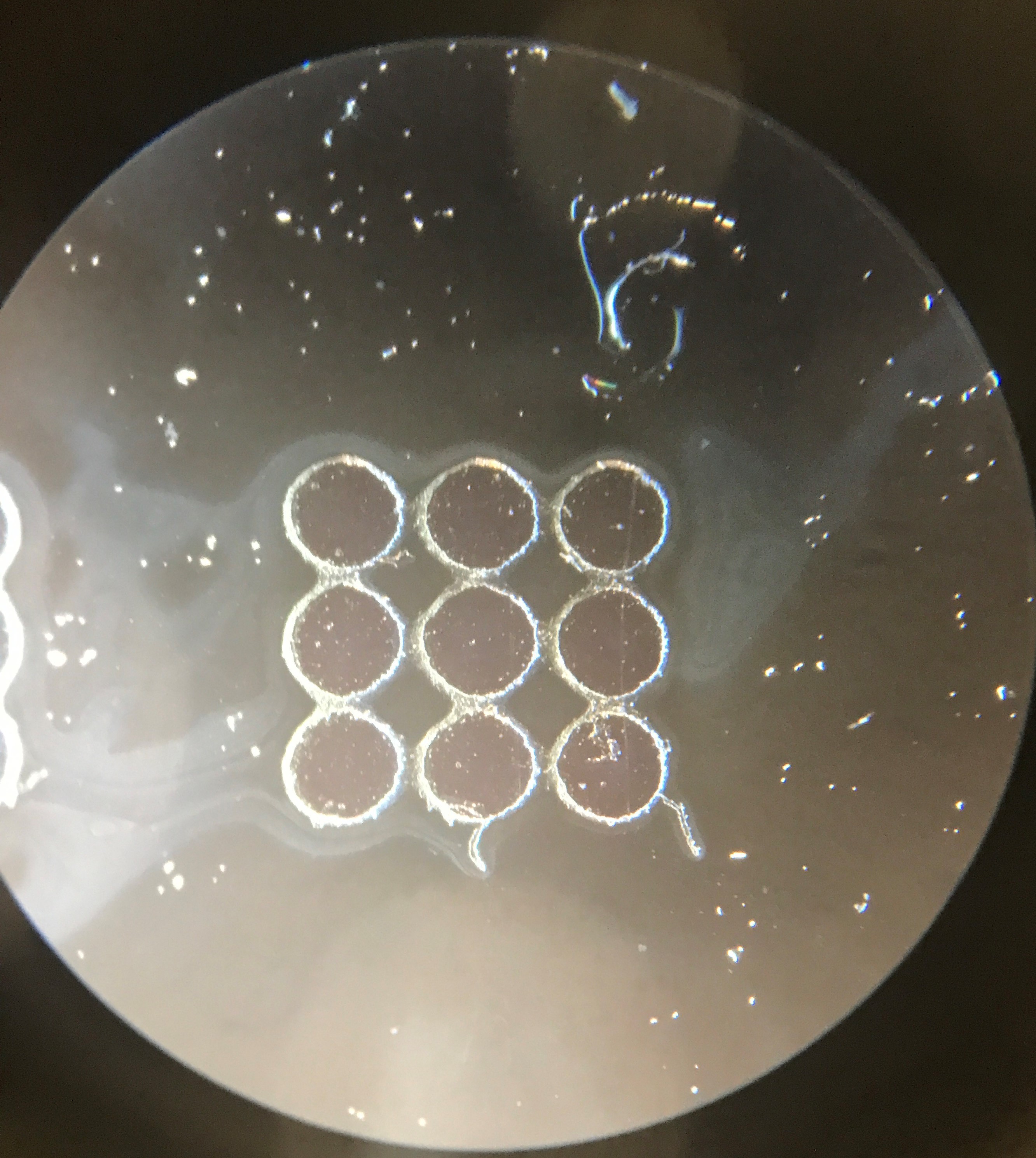
I whipped up a quick test pattern in Fusion 360 to try and get a baseline. It was just a simple set of .8 - .1mm x 20 mm channels, and then matrices of pillars of various widths and separation distances. No real hard thought went into this design, I just figured they would be good markers to see what we're working with.
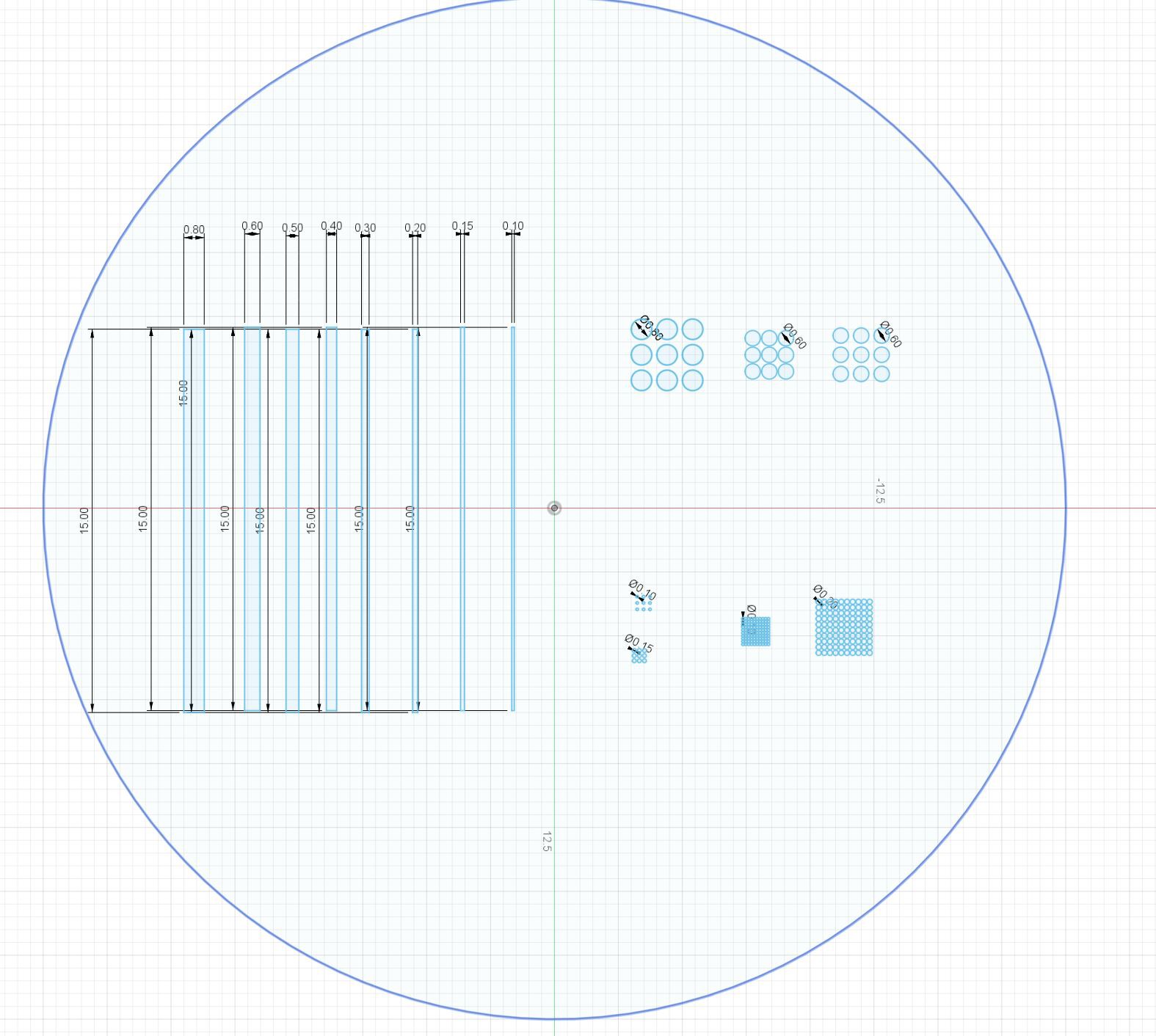
To trick the resin printer into working for this project I took the test pattern and extruded it to be 1mm thick, then set the layer size in the slicer to 1mm. This results in the LCD displaying the exposure image for whatever the single layer time is set to. I started off with a 1 minute exposure time, which proved to not be enough. Eventually I ended up around 3 minutes and was getting good results. This is going to be the first parameter I test heavily, as I suspect it will prove to be the most important.
Development:
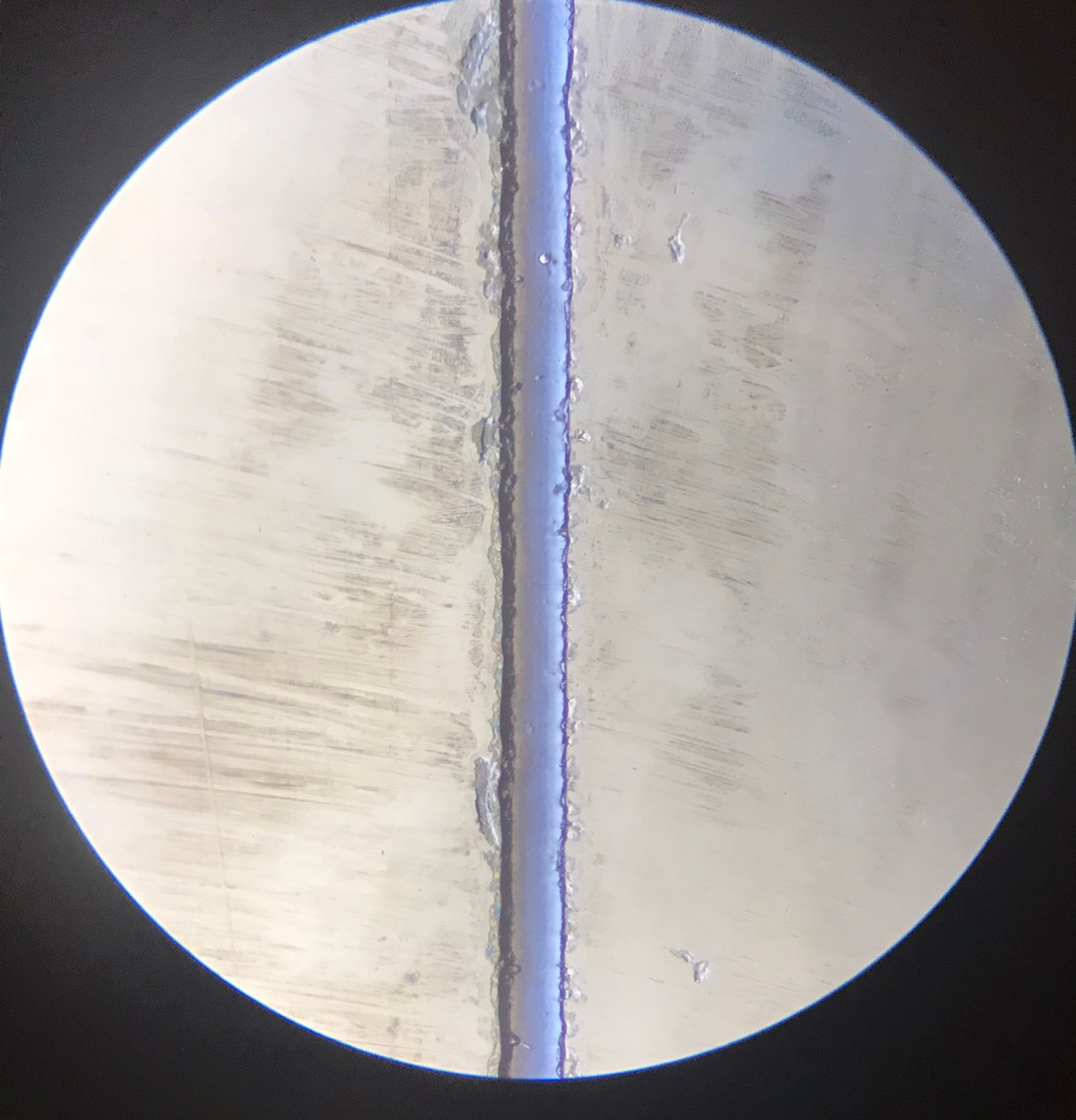
After exposure I took off the final piece of protective film from the photoresist and put the wafer into a bath with 1g of sodium carbonate to 100g water to develop. This is another really tricky spot. Leave the chip in too long and you'll wash away your channels, but don't develop it enough and you're left with extra resist in the areas you want to be bare silicon. This is going to be the second variable I try to nail down, after exposure times. I ended up leaving one chip in for about 6 minutes and it turned out okay. Definitely could be better, but for a first run these results are very promising.
Results:
I made 3 chips. One was underdeveloped, one was totally overdeveloped (all resist came off) and one was only slightly over developed (pictured below). Next steps are going to include dehydrating the silicon wafers to see if that helps with adhesion, then making some better test features to nail down the exposure and development times. During this first foray I learned a lot and can't wait to continue pushing forward. One of the principle takeaways is that I can easily remove all photoresist from a wafer using acetone, then reuse the wafer. That is going to save me a ton of time and effort tracking down surplus silicon.
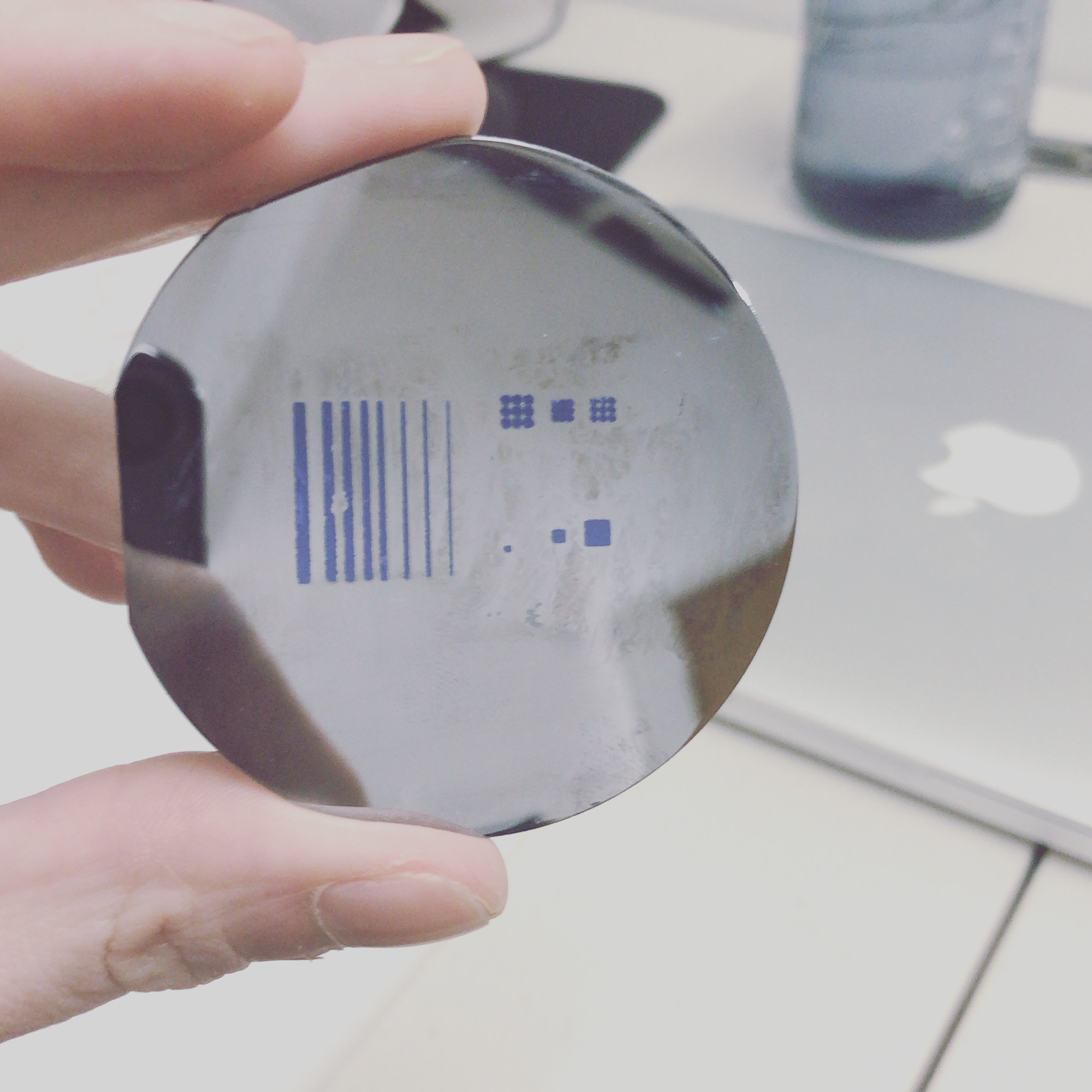
For now, enjoy these photos :)
Discussions
Become a Hackaday.io Member
Create an account to leave a comment. Already have an account? Log In.