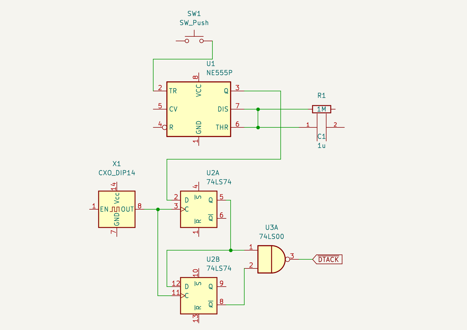
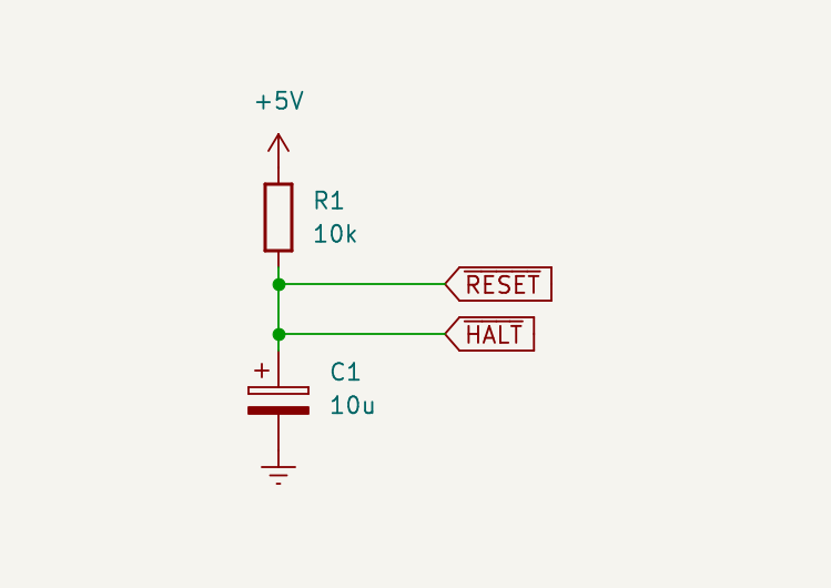
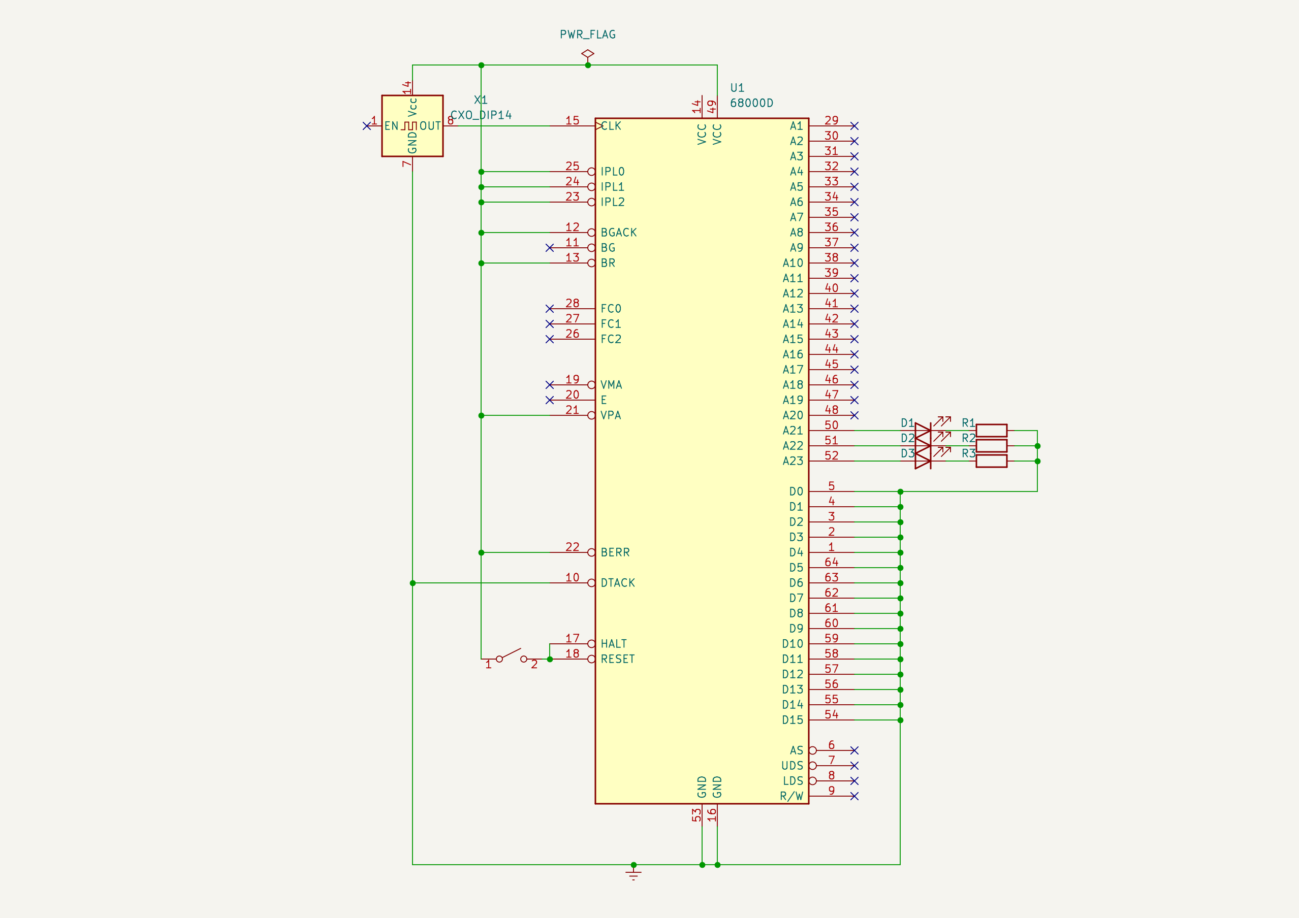
• Step 4: Step-By-Step

    Roman Romanchuk02/27/2022 at 16:01 0 comments

    I'm slowly moving forward. Trying to debug the ROM connection I achieved partial success. Still don't understand why my program didn't run like expected, suspect that bread board becoming "a bit" noisy running on 4 mHz speed, but slowing things down actually proved that connections are correct. 

    So as I don't got expected results after adding ROM, I decided that I need a debug possibility during the build. As 68000 according to data sheet have minimum clock requirement of 4mHz (my CPU is expected to run on 8mHz at full speed), I can't simple step clock. 

    There's hardware debug possibility via HALT line, but halting CPU will put address and datelines in high impedance state, so not really helping for debug. I actually don't understand how to use HALT for debug purposes, as I can not peak inside lines when CPU halted. 

    Other way is to switch DTACK from always grounded mode, emulating slow memory. This exactly what I need for debug, CPU will do nothing while DTACK become grounded keeping address and data bus active, giving me time to examine them.

    I build step scheme from two parts:

    1. Debounced button. Debouncing circuit is based on 555 monostable timer. Nice example of this circuit is provided by Ben Eater. See reference [1]
    2. Double D-latch (74LS74) circuit to provide short DTACK signal. Details of the circuit explained by John Tsiombikas in reference [2]

    As clock source I'm using oscillator connected to CPU clock input.

    Overall schematics looks like this:

    This scheme allowed me to proof that my simple loop program is executed correctly. I'm thinking a bit about extending scheme to be able to switch between manual mode and automatic (will try to find the speed on which my bread boards still able to execute correctly program), but that would be next step. 

    References: 

    [1]

    [2] 

  • Step 3: Add ROM

    Roman Romanchuk02/22/2022 at 13:03 0 comments

    The next obvious step is to add some storage with the program. 

    The first thing that I'm trying to wire is a ROM. Most of the Homebrew projects I meet recommend to use EEPROM, but I don't have a chip programmer, so made a choice to use NOR Flash instead.  I wasn't able to find any chips with 16 bit data bus, so going with pair of SST39SF chips. Simple read access able to work without any additional logic required. 

    To store program on flash I used arduino mega, it has enough pins, so I don't need to bother with shift-IC. 

    As first program I'm trying to use simple read from memory address $40000 in the loop. Idea behind - such program is small enough, so I can connect only 4 address lines to the chip, and use this high address to see LED turned on (pins A21, A22, A23 on CPU connected to LEDS as debug measure). 

            org       $08 ; initial memory location
    prg:    
    	move.w    $400000,d0 ; read from high address 
            bra.s 	  prg ; jump back to execute read in the loop 

    Compiling this program with VASM gives following byte code:

    0000000    00  00  00  00  00  00  00  00  30  39  00  40  00  00  60  f8
    0000020

    As I'm using two chips for storage, each of the odd bytes goes to the odd chip (connected to pins D0-D7) and each even byte goes to chip connected to pins D8-D15). 

    As usual happening to this project - after I wired the setup instead of 1 LED turned on I see all 3 going on and off, or just staying on. I've checked my wiring two times, found some problems, but still didn't got good enough result. 

    So I decided that next step is actually I need something that would be able to single step CPU to see that addresses I'm trying to read and what info my storage gives in response. 

    I'll post connection scheme, but not sure if it's correct, as haven't seen it working as expected yet

  • Step 2: Reset on start

    Roman Romanchuk02/13/2022 at 08:49 0 comments

    Seems i figured out that the cheapest breadboards aren't best for Homebrew computer. After switching no-name transparent boards, to elegoo (cheap "branded" ones), my binary counter is able to free run way longer than half a minute. Enough for experimentation I believe. 

    I decided to step aside from initial plan, and try to build circuit to avoid manual fiddling with wires on CPU startup. 

    Effectively this mean I need to supply power to cpu, hold HALT/RESET lines low for at least 100ms and then bring them up. 

    The simplest scheme for this would look like resistor, connection to HALT/RESET, capacitor and that's it.

    The downside of scheme - two lines bounded together, so when processor will try to operate one of them it either reset or halt. I will look a bit more detailed at reset scheme in the future, but for now it'll do fine for me. 

  • Step 1: Get free run!

    Roman Romanchuk02/11/2022 at 11:34 0 comments

    Effectively `free running` of the processor is the state where it doing something without involvement from the outside. 

    But first some basic info on the processors and execution of the code. CPU effectively doing following steps when powered on in the loop:

    1. Specify address of the command on address pins
    2. Read command from data pins
    3. Execute it

    If command execution is not influencing the address from which next command will be fetched - the next command will be fetched from next memory address. 

    The idea of `free run` is exactly this: setup minimal configuration of the chip, give to it commands to execute, and verify that address is changing after each command. One of the simplest methods of verification is to attach LED to outputs from processor that indicate the address from which next command will be changed. Usually it doesn't make sense to attach LED to every output that processor using for address, as it working fast enough, that human eye will not see flickering. So I attached the LED only to outputs A21, A22, A23 indicating 3 highest bits of the memory address, these high bits will change slow enough to see LED turning on and off.

    So how to get 68000 into free run mode? 

    According to data sheet, processor have 3 types of pins: 

    1. Input
    2. Output
    3. Bi-Directional

    First thing is to provide enough input to start processor. In case of 68000 it would mean so called `DTACK grounded` configuration:

    • Tie PIN15 to oscillator output. I'm using 4 MHz oscillator as it is minimal accepted for my 68000 chip, due to the fact that I'm building thing on breadboard, and sceptical on ability to pass high frequency signals over cheap boards I'm using. 
    • Tie PIN10 to the ground to provide "LOW" signal. 
    • Tie PIN12, PIN13, PIN17, PIN18, PIN21, PIN22, PIN23, PIN24, PIN25 to the 5V supply to provide "HIGH" signal.
    • Tie PIN14, PIN49 to 5V power supply - this chip have 2 power inputs, so supply power on both.
    • Tie and PIN16 and PIN53 to ground - each of them is ground for appropriate power input from.

    The next step would be select the command that processor will execute. Usually it's NOP, which stands for 'No Operation', but due to special startup sequence of 68000 it's not possible to use it directly. Looking on different command codes the suitable command would be 'ORI.B #0,D0'. It's not important what it's doing, but it's nice choice as binary representation of this command is: 0. So after initial sequence, processor will start reading command from data pins. As we want to give 0 there - let's tie the all data pins to ground.

    What is this initial sequence? 68000 will read first 4 words of memory and use them as address of the program to execute. By providing 0 as input during this sequence we will indicate to processor that first memory address to fetch command will be 0. 

    So after put all wires according to the scheme above, I was expecting to see a nice blinking LEDs. As it usually happens - expectation doesn't met reality and LEDs weren't blinking. 

    After starring in the datasheet and fiddling with the wires I found out that RESET and HALT lines should be down on power up and go high in some time after CPU start. According to datasheet this period should be at least 100ms. 

    So after rewiring schema and providing manual way to power up this pins at later moment (just drop that two wires on separate rail, and manually plug wire from 5V after giving power to rest) I was able to get the thing blink!

    Not sure why, but usually it stops blinking after couple dozen of seconds, but seems initial free run is success.  

    I drew schematics of free running 68000 setup. As mentioned in previous log this project is about learning by doing, so if you spot any errors or strange things in this schematics - let me know in the comments. 

  • Day 0: How it's started

    Roman Romanchuk02/09/2022 at 12:51 0 comments

    After I got mine hands on some Homebrew Z80 system, and watching some famous videos about 6502 I understood that I want to build my own thing. 

    The decision to make something based on 68000 came from unrealised childhood desire to get Sega Mega Drive system.

    I want to go step by step, not focusing on particular "retro" feeling (still will try to avoid FPGA/full microcontrollers in the build). 

    So initial build iterations I aiming are following:

    1. Get free running 68000 
    2. Wire up CPU + ROM
    3. Add UART for communications with outside world
    4. Add RAM
    5. to be continued... 

    My electronics experience is ending somewhere around Arduino with blinking LED, so I expect this project will be slow moving, depending on free time for reading books and fiddling with chips. 

    Stay tuned!