 Eric Ljungquist
The Results:
Here's a short video of the transmitter running. You may need to full screen the video to see the LCD screens at the bottom. I had a hard time getting the screens to show up on video. When the LCD backlight was on the camera had trouble with the contrast of the text. I'll have to come back to this and make a new video when I can get things to show up better on video.
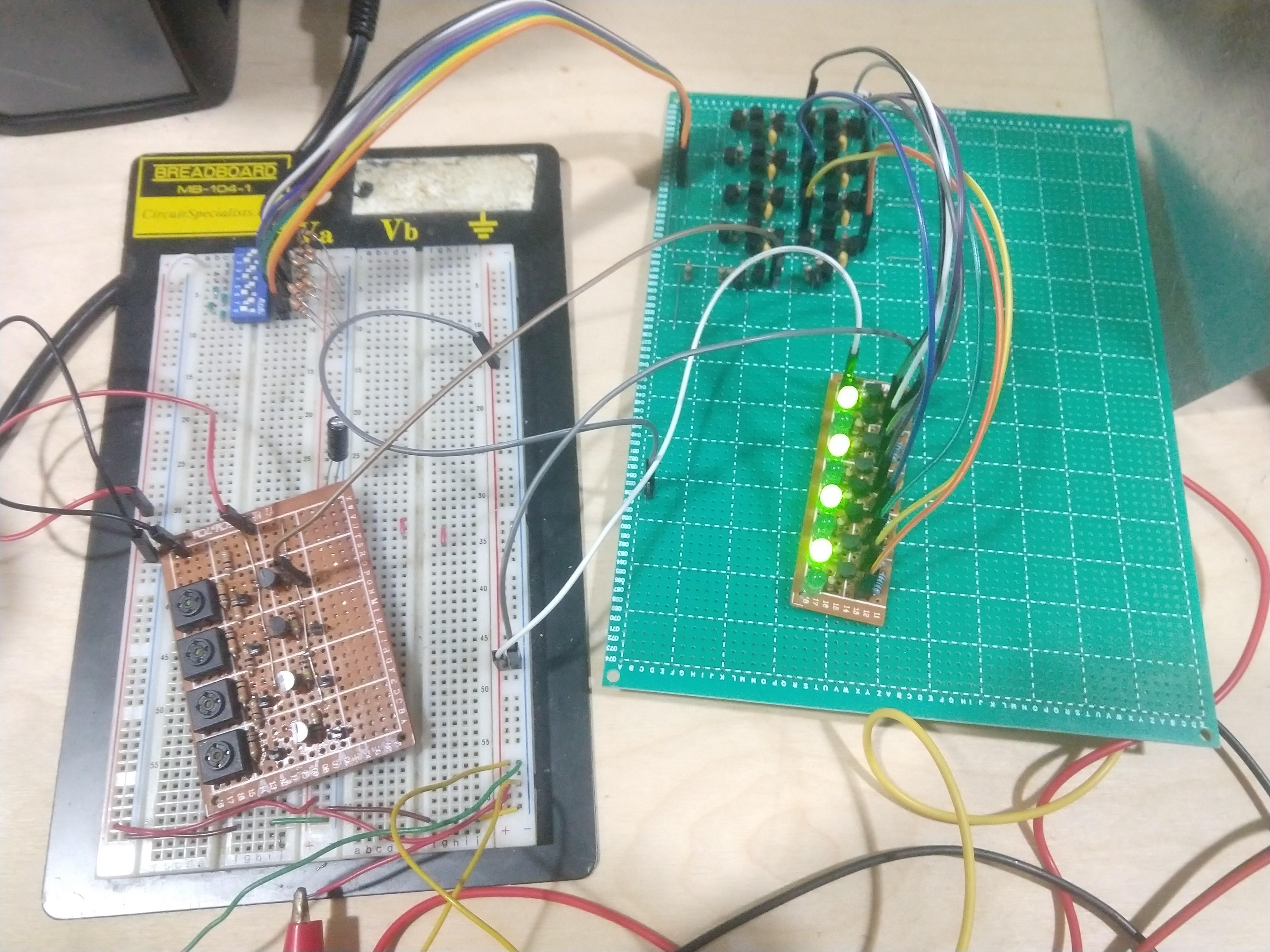
An Arduino on the left side controls the transmitter. It loops over a short list of strings and sends one of them when a button is clicked. The Arduino on the right side is set up to receive data on the Rx pin through the standard UART interface and display whatever it receives on the LCD screen.
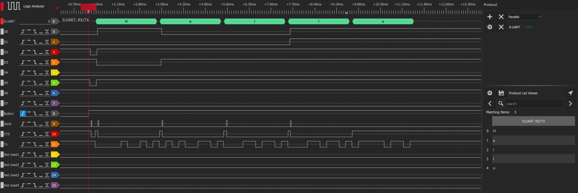
Here's a screenshot from DSView showing a live test where I sent the string "Hello". D0-D7 and Send(aka. Load) are the important inputs and Tx is the serial output. The DSView software is able to automatically decode the Tx signal that was generated by the project as what was intended.
The Design:
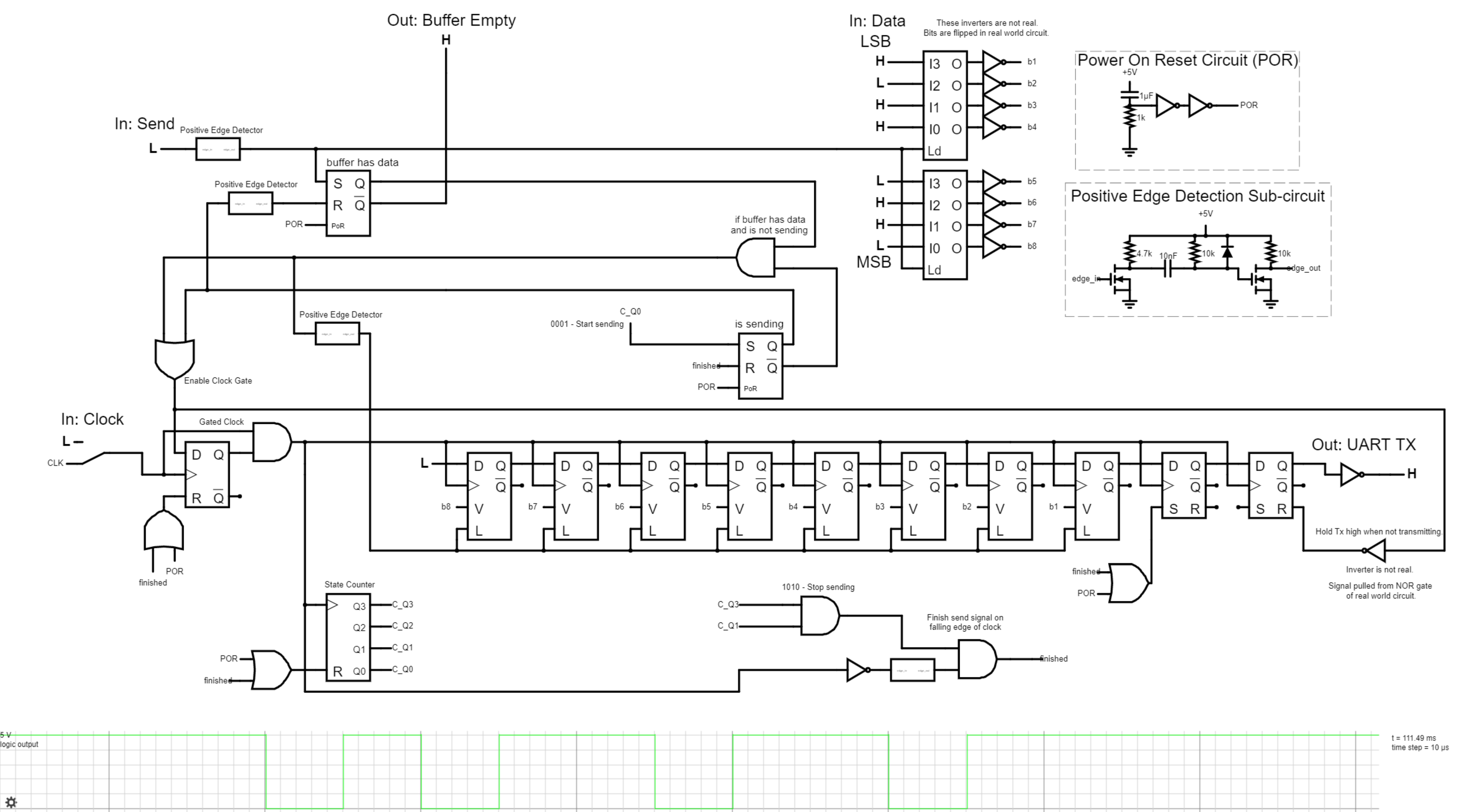
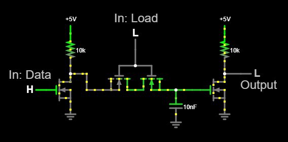
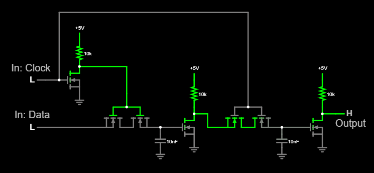
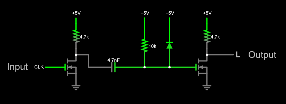
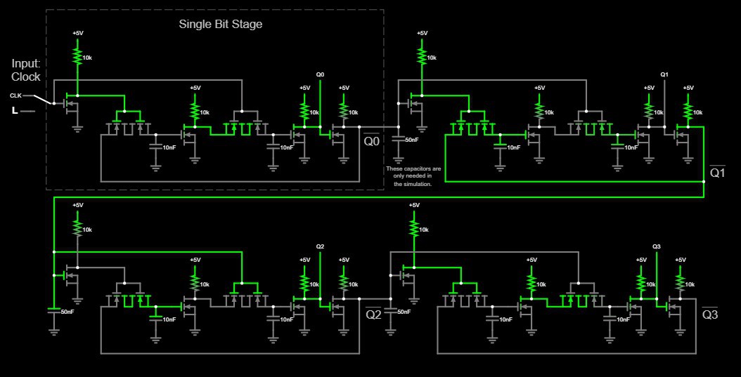
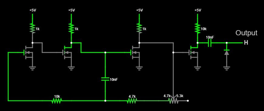
I came up with the design by messing around in Paul Falstad's CircuitJS. I kept adding parts to and refining the simulation until I had something I liked. To start, I knew I needed a Parralel-In-Serial-Out shift register to structure the output signal. From there I added a state counter and clock input. About halfway through the design I decided that it would be a good idea to include a buffer that was at least one byte. The
Whenever I added something new to the design I would stop working on the simulation and come up with an NMOS solution that worked as a real world circuit to match what I needed.
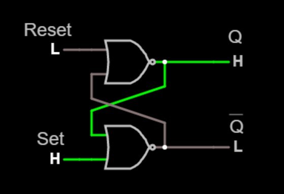
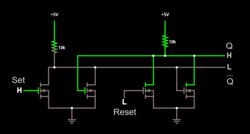
I heavily relied on dynamic logic to reduce the parts count of any sequential circuits. The only time I used the static logic version of a circuit was with the SR Latches as they only took 5 transistors to implement anyway.
Check the Project Logs for more details about sub-sections of the project.
The Construction:
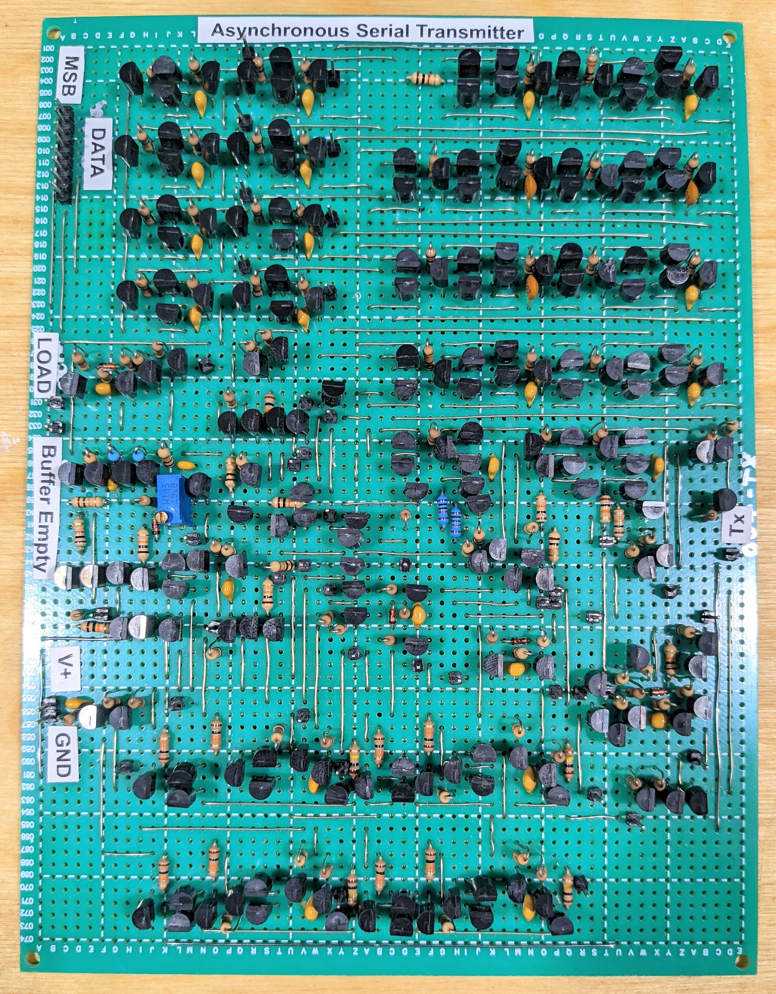
I wanted to maintain a sort of an IC layout sort of feel to the project and so I avoided using air wires or using point-to-point wiring. I made an exception for straight wires on the top layer as I couldn't find a double sided perfboard at this size. Everything is connected only on the top and bottom layer.
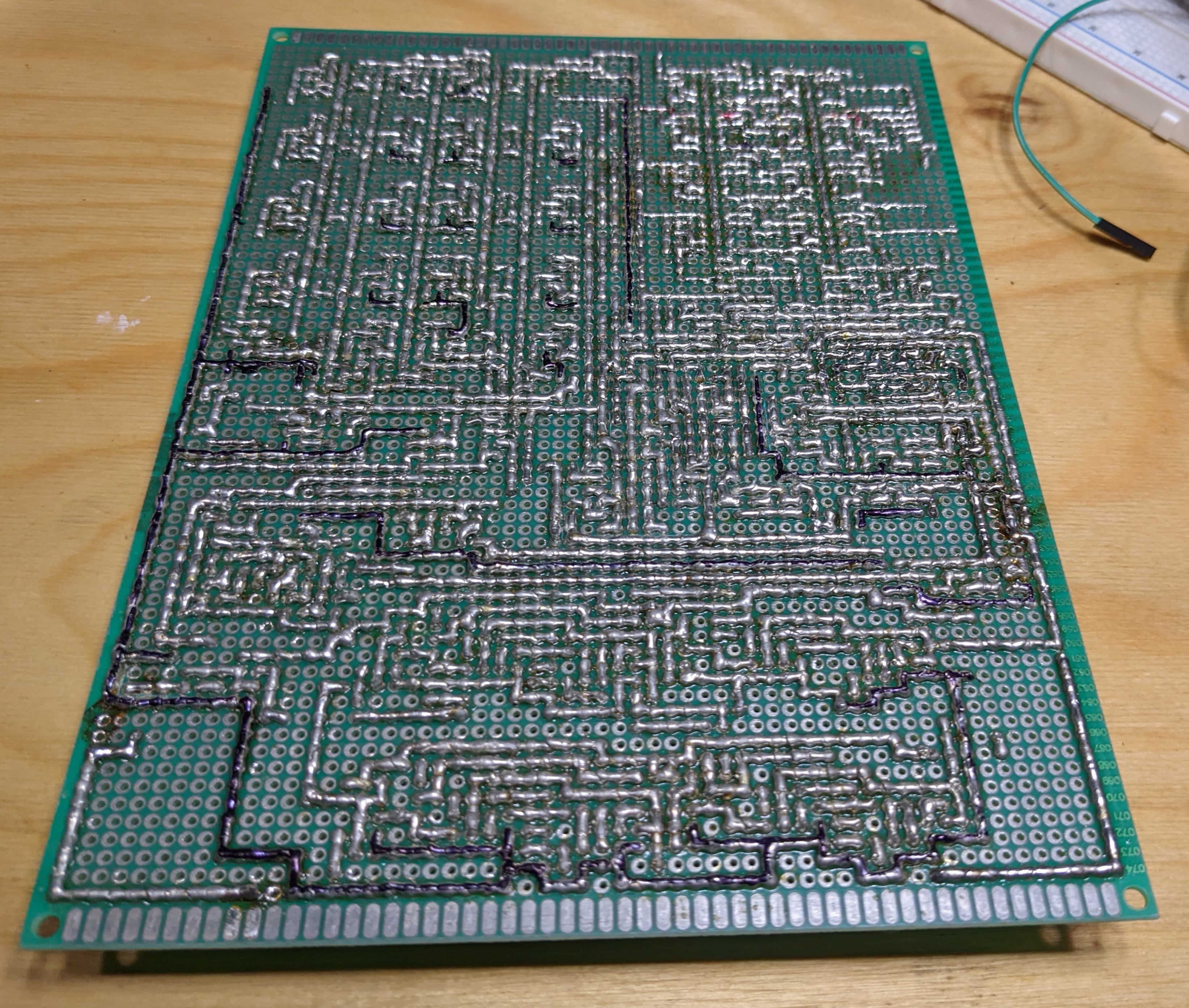
I used solder bridging on the backside to connect components together. In the beginning I used thin wires to make it easier to bridge between pads but I would recommend against it. The embedded wire made it difficult to desolder when I had to go back and make a few changes.
I ended up using nearly an entire 100g roll of solder for this project. The solder contracting after cooling actually caused the entire board to warp slightly.
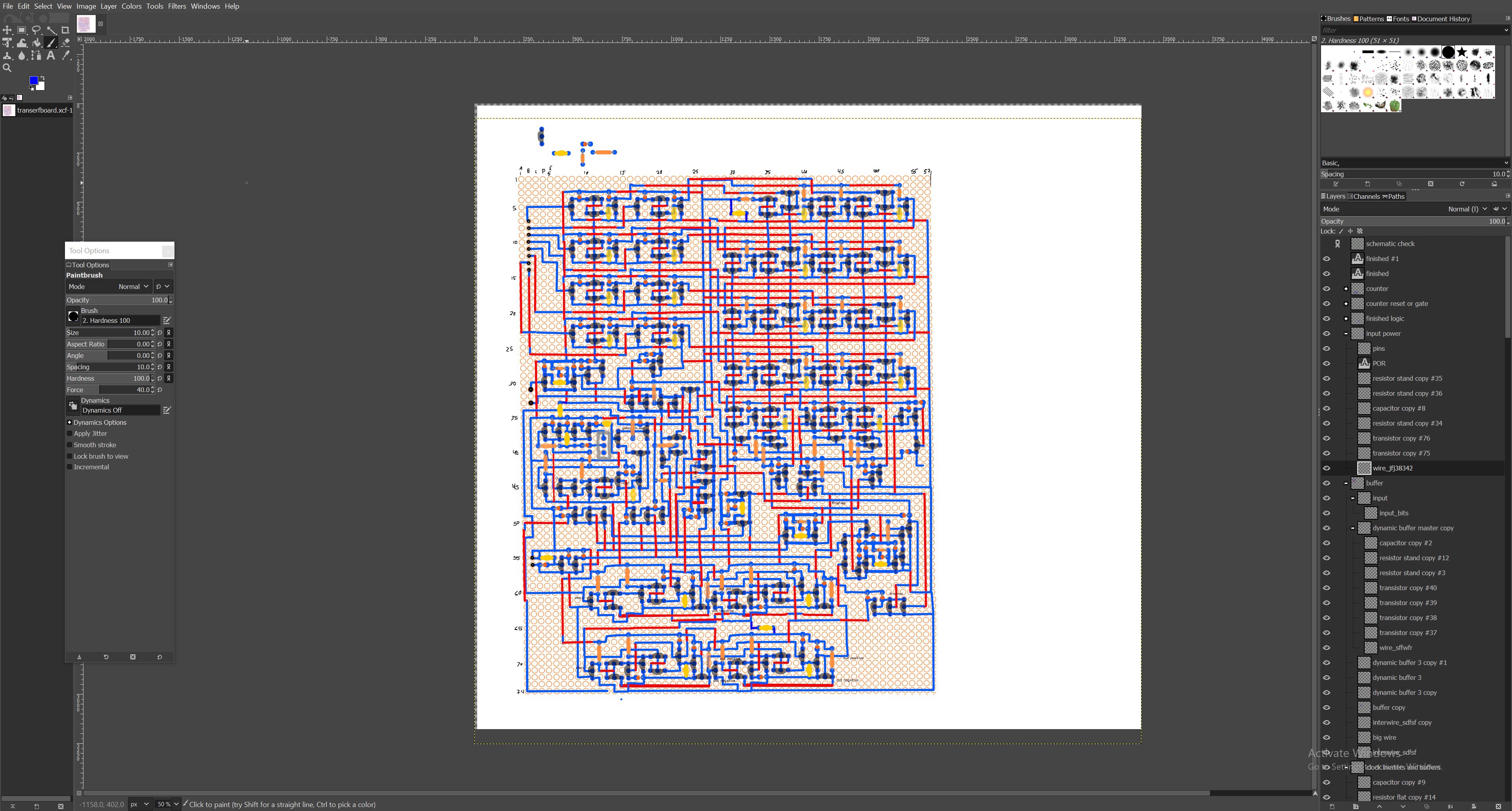
I quickly realized that I would have to come up with a way to preplan the layout on the board. I didn't know how large subsections of the circuit would be and how they would all fit together. I wanted a way to be able to move components around so that I could experiment with finding the most space efficient layouts that I could come up with.
I started off in Microsoft PowerPoint since I could draw and move around shapes easily. With the number of shapes growing quickly for just the first D Flip-Flop in the counter, PowerPoint was acting unwieldy. I needed to switch to another solution. I didn't end up finding a perfect fit of some kind of perfboard layout tool and I went back to my fall back option. GIMP. I could drag around shapes but layers and groups let me organize things while allowing me to easily move parts around.
I made a grid of dots to represent the grid of holes in the perfboard and drew a few components to match the size on the real board. GIMP was able to handle a huge number of layers without getting laggy to user input but did use a large amount of memory by the time I was finished the layout. The only big drawback was drawing the wires. If I wanted to make a big change to...
Read more »


 matseng
 Tim
Tim
 Dave Collins
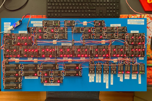
 Joël de Kanter
Very cool project, lot to learn from about discrete implementation of logic gates! I am just wondering, given that the 8-bit output word needs to only be stored during the time to send (which is short even for slow baud rates), if 8 capacitors could be used as "memory cells" - first tied to bus, and then to output mux (I used mux instead of shift register to generate TXD, see here: https://hackaday.io/project/181664-intel-hex-files-for-fpgas-no-embedded-cpus/log/197809-par2ser-a-novel-uart-transmitter-counter-driven-mux-approach ). 9th capacitor (same as other 8) with some "level sense" circuit could be used to signal to host CPU when 8 others are charged (like /WAIT signal at writing to output port). At the moment of sending the bit (mux selection to TXD) the capacitors would be also discharged.