 Nate Rivard
This project assumes you know about or have used SPI in some form or another. This could be with an AVR, a Raspberry Pi, or bitbanging it to a peripheral using your own 6502 design like me. This project is also focused on building a circuit for use in a very specific device: the n8 Bit Special microcomputer. This means that certain design decisions will be made to gracefully interoperate in its eventual home.
SPI
As a most basic refresher, SPI is a full-duplex serial data protocol with one orchestrator device and potentially many peripheral devices sharing some common control lines but individual device enable lines. Data is moved 8 bits at a time between orchestrator and peripheral. A typical hardware example illustrates this using 2 shift registers: one in the orchestrator and one in the peripheral, forming a circular buffer:
There are also 4 modes, each of which describes when data is sampled in which device. For details on this (and more), you can check out the SPI Wikipedia page.
Bit Banging SPI
SPI is a pretty simple protocol so its often "bit-banged": using software and some simple control lines to communicate instead of dedicated hardware. This has some disadvantages though: it's pretty slow (it's going to be significantly slower than your CPU's clock. I was able to get it to about 60khz but the CPU clock was 2Mhz!) and your CPU is dedicated entirely to the task until it's finished. It may also take a significant percentage of your computer's GPIO capability, especially with more than one device.
SPI on AVRs
AVRs have solved this by building SPI support directly into the chip itself. This hardware is exposed via 3 registers: a data register, a status register, and a control register.
The data register is a read-write register. Writing to it initiates an SPI transfer and the data received is stored in a buffer which can be read.
The control register is a read-write register for configuring various SPI modes, roles, and speeds. It looks like this:
| Bit 7 | Bit 6 | Bit 5 | Bit 4 | Bit 3 | Bit 2 | Bit 1 | Bit 0 |
| SPIE | SPE | DORD | MSTR | CPOL | CPHA | SPR1 | SPR0 |
SPR0 and SPR1 form a 2 bit clock rate divider.
CPOL and CPHA form a 2 bit mode select.
MSTR is a bit to control whether the AVR is the master or a peripheral.
DORD is a bit to specify data order (MSB vs LSB).
SPE is an SPI Enable bit.
SPIE is an SPI Interrupt Enable bit.
The status register only has 3 relevant bits, and looks like:
| Bit 7 | Bit 6 | Bit 5 | Bit 4 | Bit 3 | Bit 2 | Bit 1 | Bit 0 |
| SPIF | WCOL | x | x | x | x | x | SPI_2x |
SPI_2x is a bit to double the speed (it basically forms a 3 bit clock divider)
WCOL is a read-only bit if there a write collision occurs. In other words, if data is written to the data register while a transfer was already in progress.
SPIF is a read-only bit that is set when a transfer is complete and is cleared when SPIF bit and data register are read.
The AVR also has some dedicated SPI control lines: MISO, MOSI, CLK and you can use any GPIO pins as device select lines to your peripherals.
SPI Master
I want to achieve something very similar for my microcomputer. I want dedicated hardware that appears as exposed registers that perform SPI tasks and notify me when they're done. I also want to do this in discrete logic. Could I build this in an FPGA? Sure. Can I also just use an AVR and use its dedicated SPI hardware? Sure. But I don't want to :)
So, how will I achieve this? Well, first I actually shed some of the requirements. My design will not have any mode select, it's going to be Mode 0 only. I'm also going to (for now) skip things like double speed and write collision.
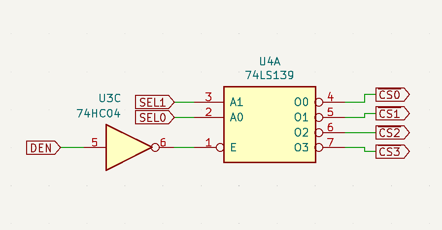
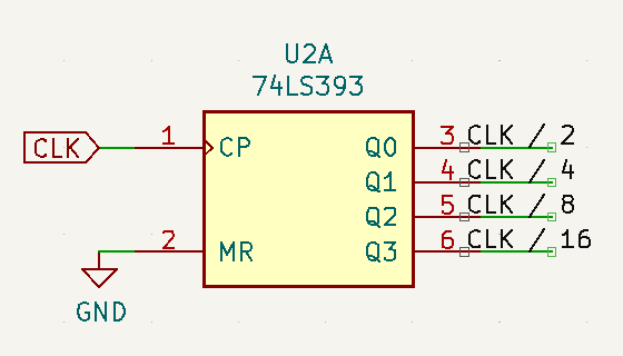
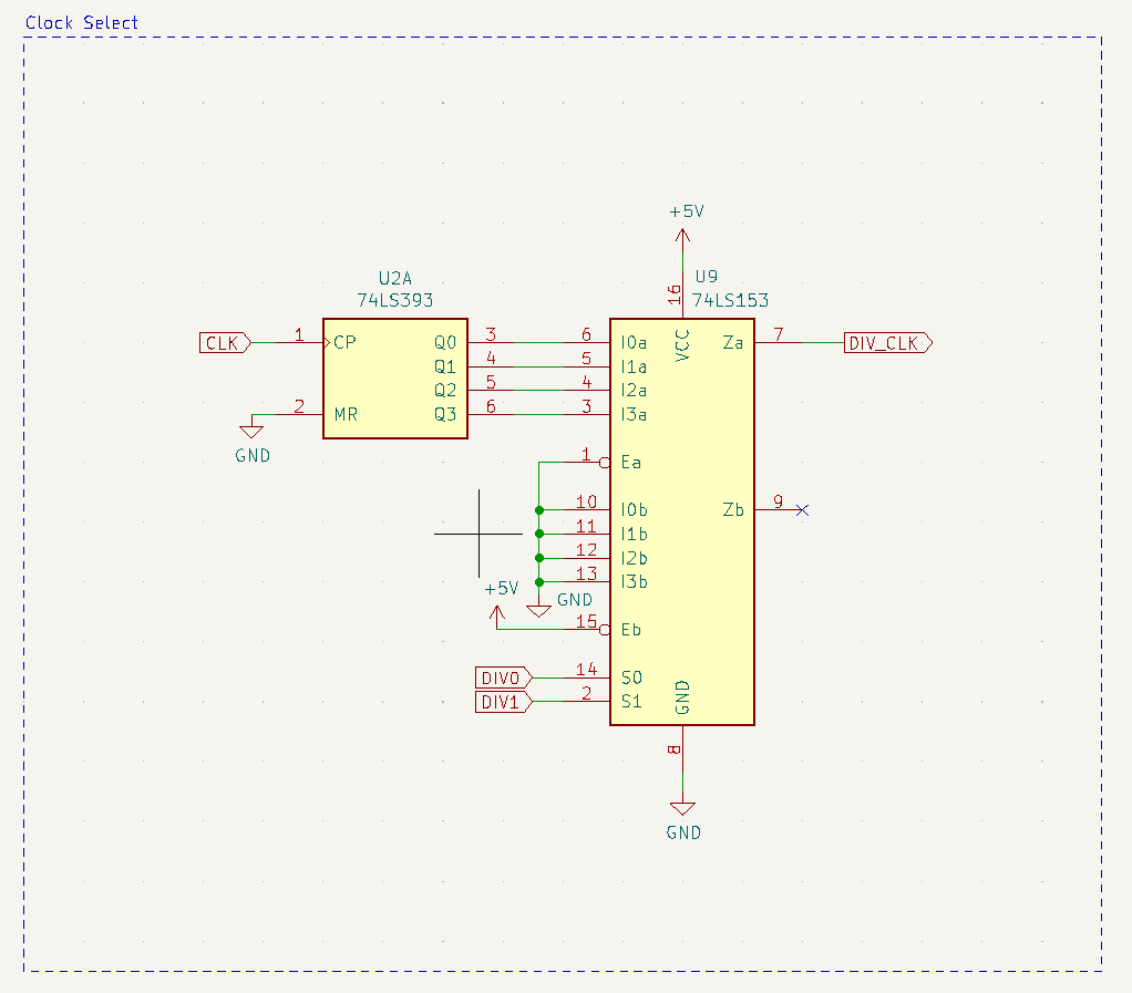
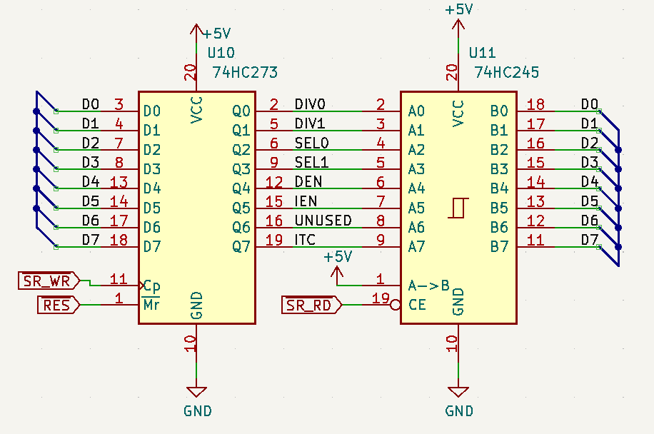
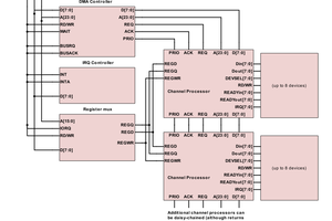
Next I'm going to add to the requirements. SPI master will have hardware to control up to 4 SPI devices. The 6502 doesn't have any built-in GPIO and I don't want to dedicate VIA pins to this purpose so it makes sense to build this in.
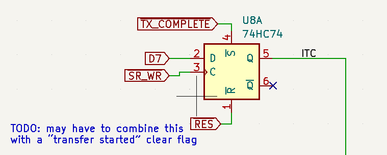
The rest of the requirements remain: I want clock speed selection, I want interrupts, I want a set it and forget it data register that initiates...
Read more »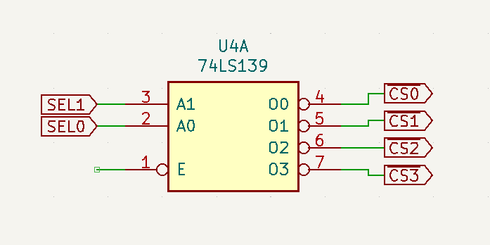
 Dave
Dave