Nate Rivard
-
Part 3: Device Select
07/13/2022 at 11:17 • 0 commentsOverview
In keeping with our theme of understanding the control register, we will look at the device selection and device port subsystem.
In SPI systems, the orchestrator and many peripherals share some common lines (MOSI, MISO, CLK) so there needs to be some mechanism to signal which peripheral is the intended target of communication. In our control register, we have 2 bits dedicated to selecting 1 of 4 devices, SEL0 and SEL1:
SEL1...SEL0 Selected Device 00 0 01 1 10 2 11 3 We also have one bit in our control register to turn off all devices. When DEN is HIGH, the device targeted in SEL1 and SEL0 is asserted and when DEN is LOW all devices are de-asserted. In other words, no peripheral should be listening anymore.
Design Considerations
This subsystem is fairly straightforward, but we still need it to:
- select 1 of 4 possible devices via software
- be able to completely de-assert all the devices or assert a single device via software
- have some mechanism to connect devices to this circuit
Design
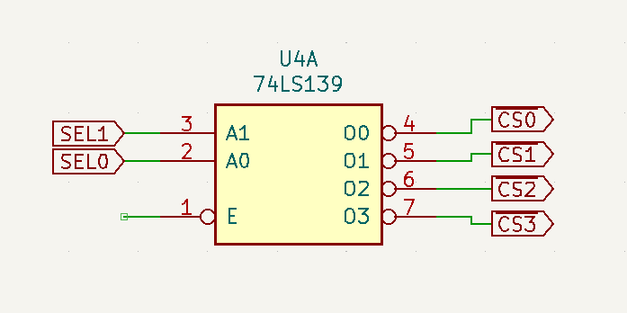
We will start by selecting 1 of 4 possible devices. We have already looked at using a 2-to-4 mux in our clock select circuit. This device takes 4 input lines and selects 1 of those lines as output via 2 select lines. Our device select logic, though, should actually be the opposite: we have a single "input" (we will discuss this later) that we want output on a single line out of a possible 4 lines. To accomplish this, we will use one half of a 74HC139 Dual 2-to-4 line decoder/demultiplexer (don't worry that the diagram states a 74LS139, it's being used here because it has the same footprint and function).
![]()
You may have noticed the deliberate usage of "assert" and "de-assert" when referring to turning on or off a device. This is because SPI is active-low to assert a device, not active-high. That means for our demux, our input would actually be a constant LOW signal and that LOW would flow out to the selected device. One nice feature of the '139 is that "input" is already assumed.
We also need a way of de-asserting all devices. In other words, we want all of the outputs to be HIGH. Another feature of the '139 is that it has an active-low ENABLE pin. When E is HIGH, all the outputs are HIGH. When E is LOW, the line selected via A0 and A1 is LOW.
The intended method of controlling this is to use DEN. One consideration here is that on bootup, RES will go low and we want our control register to be reset. The 74HC273 we're using will zero the itself out, which means a LOW signal will be the default for DEN.
If we connect that line straight to E on our '139, it means a device (in this case Device 0 bc SEL0 and SEL1 will also be reset as LOW) will be asserted! This could be very bad as we don't know what will be on some of our other lines like CLK, MOSI or MOSI. So ideally, we want a LOW on DEN to mean de-asserted and a HIGH to mean asserted.
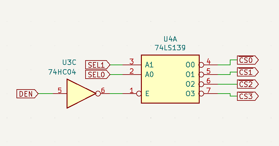
To do this, we will use one-sixth of a 74HC04 Hex-inverter. So our final design for the device selection logic is:
![]()
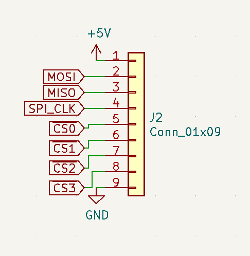
Lastly, we need a way to route our signals to actual devices. A simple and flexible way to do this is to provide a user port on the board. We haven't talked about some of the signals referenced in this circuit, but here is our port:
![]()
It provides 5V power and shared GND (only GND is truly necessary here. Devices can be self powered if they want to), MOSI, MISO, and SPI_CLK (these will be discussed when we talk about the data register) and our 4 device select lines.
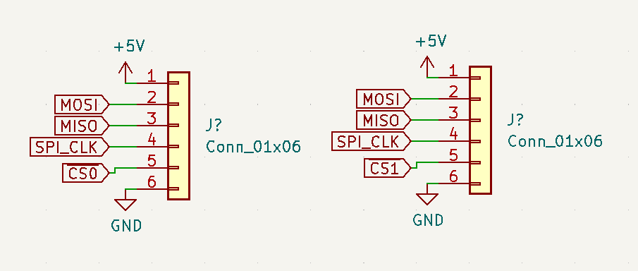
One interesting and perhaps nice change would be to provide 4 almost identical ports:
![]()
Here our shared lines are in identical spots across two ports but they each have a separate device select line routed. This would allow us to standardize connectors for our devices and provide power and ground to each device.
But for now, we will go with a single 1x9 port!
-
Part 2: Clock Select
07/01/2022 at 10:28 • 0 commentsOverview
The next subsystem we're going to examine is the clock select logic. SPI orchestrators and peripherals all share the same clock, generated by the orchestrator, to stay in-sync. Peripherals may only accept specific ranges of frequencies so the orchestrator needs the ability to generate a wide range of frequencies for better compatibility.
Remember that in our control register we dedicated 2 bits (so 4 possible values) to clock selection: DIV0 and DIV1 (Note: the target system for this device, the n8 Bit Special microcomputer, has a main clock of 3.6MHz):
DIV1...DIV0 Result Value @3.6Mhz 00 CLK / 2 1800 kHz 01 CLK / 4 900 kHz 10 CLK / 8 450 kHz 11 CLK / 16 225 kHz One side effect of this is that it is impossible to run the device at the full speed of the main clock.
Design Considerations
As previously stated, SPI peripherals may only accept specific ranges of clock frequencies and these limits are typically at higher clock speeds. SD cards, for example, can only be initialized in SPI mode under 400khz. Afterwards, they operate just fine in the Mhz range. With that in mind, this clock selector should be able to:
- operate under 400khz
- change clock speed via software
Design
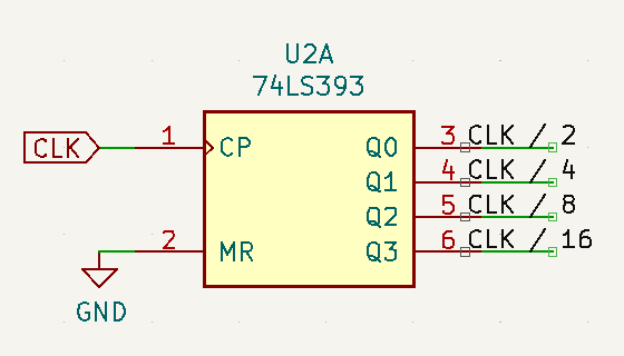
We will start with the circuit to generate our 4 possible clock values: the main clock divided by 2, 4, 8, and 16. You may see a very useful pattern emerge if you stare at those values long enough. Each value is half of the previous!
We will use this property to efficiently generate our divided clock signals using one half of a 74HC393 4-bit binary ripple counter. We will connect our main system clock to the clock input of the counter and each of the 4 outputs will be our 4 clock signals:
![]()
Note that we tied MR line to ground (this reset line is assert high!) so this counter will run continuously and cannot be reset. This has the potential side effect of the first pulse of the divided clock being too quick after changing the clock speed but this doesn't seem dangerous.
This device is also negative-edge triggered rather than positive-edge triggered like many of the other devices in this design. On integration, we will see if that is going to be a problem or if we will have to invert the incoming clock signal to better fit.
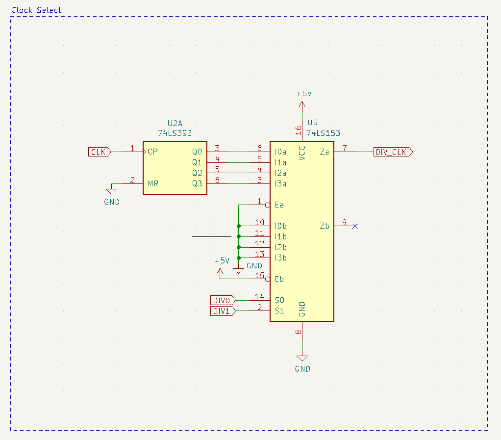
Now we need a way to programatically select which of these signals is our divided clock, using the 2 lowest bits in our control register. For this we will use one half of a 74HC153 4-input multiplexer. In essence, this allows 2-lines to select a single line from our 4 inputs, exactly what we need. The other half of the device is just completely disabled so there is no interference. So our final design is:
![]()
-
Part 1: Control Register
06/29/2022 at 15:48 • 0 commentsOverview
We will start our discussion of this design with the control register because virtually every other subsystem depends on it in some way. It is the primary interface for controlling the behavior of the device. To recap, the control register is an 8-bit read/write register and this is how its bits are laid out:
Bit 7 Bit 6 Bit 5 Bit 4 Bit 3 Bit 2 Bit 1 Bit 0 ITC x IEN DEN SEL1 SEL0 DIV1 DIV0 - DIV0 and DIV1 are a 2-bit clock divider select
- SEL0 and SEL1 are a 2-bit device select
- DEN is a device enable flag
- IEN is an interrupt enable flag
- Bit 6 is unused
- ITC is a transfer complete flag (it is also an interrupt acknowledge flag if IEN is enabled and a transfer has completed, thus triggering an interrupt)
Design Considerations
There are a few things to remember when designing this control register:
- it needs to fit in well in a 6502 memory-mapped environment
- it must be safe to read and write
- it must be resettable
- other subsystems are controlled via flag values so these have to be accessible to the rest of the design without driving the shared data bus
- on a completed transfer, the ITC flag (discussed in a future log entry) must be automatically set. This requirement causes much of the complexity of this design
Design
In discussing the design, we will add complexity layer-by-layer to address each of the design considerations.
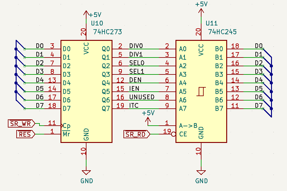
To start, we need a read/write register that fits well in a 6502 memory-mapped environment. For this basic task, I chose a 74HC273 Octal D-type positive-edge triggered flip-flop. This IC satisfies the first 2 considerations pretty well. It features:
- 8-bit input/output
- dedicated reset line
- data latch on a positive-edge trigger to its clock line
Unfortunately, this device by itself does not fit well in a 6502 memory-mapped environment. When SPI Master is not being addressed, it should be completely disconnected from the shared data bus. This particular chip doesn't have that capability.
One option is to use a 74HC373. This device has built-in tri-state buffers that can prevent the IC from driving the data bus, but this would break the requirement that other subsystems be able to read flag values when the device isn't asserted.
The solution I've chosen is to use a 74HC245 Octal bus transciever. The '245 is configured to permanently flow in one direction, A -> B, where A are inputs and B are outputs. Next, the '273 outputs are connected to the '245 inputs, and the '273 outputs are connected to the shared data bus.
![]()
Other devices can connect to the lines between the two ICs, thus satisfying that design requirement.
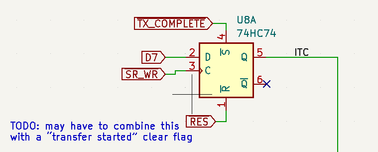
Only one requirement remains, which is the ability to set/reset the ITC bit independently. This requirement is the most complex because in many cases, to the system, it should just look like a regular 8-bit register. You write values to it, you can read that value back. But in certain scenarios, when a transfer is complete (and potentially when a transfer is started), the ITC bit should be set (or cleared, respectively) by the device itself.
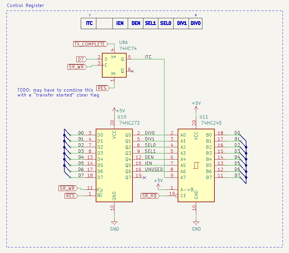
To satisfy this design requirement, I've chosen to break the top bit out into its own device, one half of a 74HC74 Dual D-type positive-edge triggered flip-flop. This flip-flop has separate set and reset lines and is triggered at the same time (when their clocks are connected to the same signal) as the '273.
![]()
On startup, the RESET line is driven low and the value is 0. When a transfer is complete, TX_COMPLETE is driven low and the value is set to 1. Otherwise, the user can write a value to it on D7 as part of a memory write or can read the value on D7 as part of a memory read.
This could bring a potential failure point (or quirk at least) because you can write a 1 to this bit and tell the device "transfer is complete". This would kick off an interrupt if enabled, etc. One solution to this is to disconnect D7 from the input side, but you would need a way to acknowledge an interrupt and clear ITC from the programmer's perspective. The venerable 6551 ACIA does this by clearing the interrupt flag when the data register is read. That is something to explore, but for now, the programmer can clear ITC (and thus acknowledge the interrupt was handled) by writing a 0 to this bit in the control register.
Putting it all together, this is the "final" design for the control register.
![]()
Q7 from the '273 is disconnected from the '245 and instead Q from the '74 is connected. We will address the 2nd half of the '74 and how the various signals referenced (SR_WR, SR_RD, TX_COMPLETE) are generated in later posts.
SPI Master
An SPI interface for 6502 microcomputers using discrete logic gates