Close
0%
0%

AOZORA

home-brew 16-bit computer on breadboard

Similar projects worth following

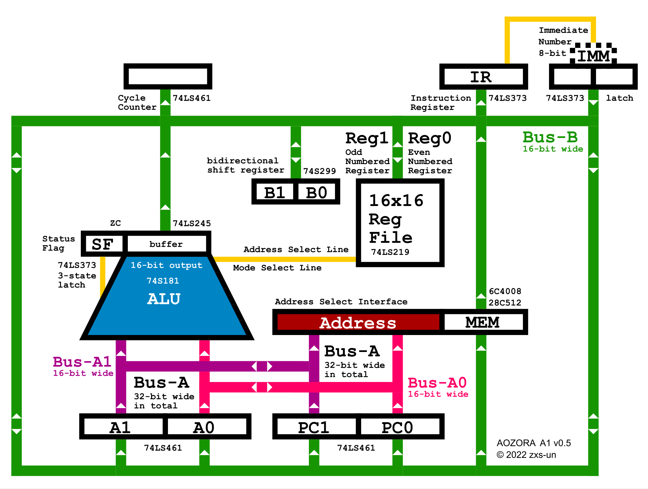
The AOZORA project aims to implement a 16-bit computer with mainly 74-series TTL ICs on solderless breadboards, providing an open and easy platform for educational purposes.

"AOZORA" is an acronym for "Allgemeine Ordentliche SOgenannte RechnenAnlage", which means "general-purpose well-organized so-called computing machinery". AOZORA may also be transcribed as Japanese Romaji to Kanji (漢字, Chinese characters) "青空".

A1 features:

  • Load-Store Architecture
  • 16 general-purpose registers
  • 16-bit word length
  • 32-bit address space (4G)

  • Revision of Bus Architecture for A1

    zxs-un04/07/2022 at 15:40 0 comments


    Bus Architecture for A1 v0.5

    The previous bus architecture turned out to be too complex to implement on breadboard. So here comes the new version. The microcode set would be updated later on.

  • Microcode Design in Progress for A1 with a Newly Modified Bus Architecture

    zxs-un03/16/2022 at 09:58 0 comments

    The targeted decoding ROM is going to have 8-bit output. Under such restriction, the number of microcodes has to be not grater than 2^8 = 256 = 16 x 16.

    Operation / Data Flow
    Coding Space
    Comment
    B < B1 < Bus-C < Reg
    B > B0 > Bus-B > Reg
    2 x 16Totally 16 registers in reg-file
    A1 < Bus-C < Reg
    A0 < Bus-C < Reg
    2 x 16
    B < ALU < Bus-A < A1A0
    2 x 16
    74LS181 has 5 lines selecting
    2 modes by 16 functions
    PC1 < Bus-C < Reg1

    PC0 < Bus-C < Reg0

    1 x 16
    PC1 may only be loaded with
    odd numbered registers. 1 x 8
    PC0 may only be loaded with
    even numbered registers. 1 x 8
    PC1 > Bus-A > ALU > B >> Reg1

    PC0 > Bus-A > ALU > B >> Reg0

    1 x 16

    MEM < Bus-C < Reg
    MEM > Bus-B > Reg
    2 x 16

    C1C0 < Bus-C < Reg
    1 x 16
    D1D0 > Bus-B > Reg1 x 16

    SL(B)1
    SL(B)0
    SR(B)1
    SR(B)0
    4Shift Left (B) one bit and fill 1
    Shift Left (B) one bit and fill 0
    Shift Right (B) one bit and fill 1
    Shift Right (B) one bit and fill 0
    0(ALU) > B1 > Bus-C > MEM
    1(ALU) > B1 > Bus-C > MEM
    0(ALU) > B1 > Bus-C > C1C0
    1(ALU) > B1 > Bus-C > C1C0
    4All bits with 0
    All bits with 1
    Generated by ALU 74LS181
    C1 > D1
    C0 > D0
    C1 > D0
    C0 > D1
    4
    IO < C1
    IO < C0
    IO > D1
    IO > D0
    4
    IMM > D0
    IMM > D1
    2

    IMM > IO1
    0(ALU) > B > Bus-B > CycleCounter
    1
    Reset CycleCounter to 0
    StatusFlag < Bus-B < B0 < B
    1
    IR < Bus-B < MEM
    1Fetch instruction from memory
    A++132-bit {A1, A0} increase by 1
    PC++132-bit {PC1, PC0} increase by 1
    number of microcodes in total216
    = 6 x 2 x 16 + 4 x 4 + 2 + 6

    An extra "SILENT" operation, to silent all buses and control lines, with the ClockCounter still working increasing, might also need be coded.

    The bus architure has been modified again to make coding in 16x16 feasible. Also smaller number of ICs is preferred.

    A1 bus architecture v3
    Fig. Bus Architecture v3 for A1

  • Design Progress in Bus Architecture for A1

    zxs-un03/12/2022 at 18:59 0 comments

    With just a flash in mind, being not a professional and starting from zero, after 3 weeks of search and learn, the bus architecture design for A1 finally came out.

    At the very first beginning, project AOZORA was targeted to implement the Ibex RISC-V RV32EC core with mainly 74-series TTL ICs on solderless breadboards. 

    After reading project Pineapple ONE, support for RV32EC was abandoned, since a 32-bit computer requires a lot more ICs than a 16-bit or 8bit computer, as well as the 32-bit bus might be too wide to implement on breadboards.

    Data bus width was finally decided to be 16-bit, and address bus to be 32-bit.

    First version of the bus architecture design for A1 is mainly inspired by the famous 6502, and was hugely influenced by load-store architecture commonly seen in RISC architectures.

    A1 bus v1
    Fig.1: Bus Architecture for A1, version 1

    Just one day after the bus architecture idea on paper has been redrawn with software, when reading amazing home-brew computer projects on Hackaday, 2-Zons' project 8 Bit Breadboard CPU showed at SIMILAR PROJECTS.

    After looking into the block diagram of that project, it is clear that A1 shares a very similar bus architecture with that project.

    So the bus architecture for A1 got some refinement inspired by that project and thus comes the second version.

    A1 bus v2
    Fig.2: Bus Architecture for A1, version 2

    Bus architecture design is now almost complete, though a comparator might be needed alongside the ALU and the address decoder might also need design in detail. Focus will be put on designing controller unit and instruction set then.

View all 3 project logs

Enjoy this project?

Share

Discussions

Similar Projects

Does this project spark your interest?

Become a member to follow this project and never miss any updates