Introduction
The name of DIM-110 came from the Digital Inspection Microscope and the 110 is the work size of the X-Y axes so it is 110mm.
I was into microscope for years now and always wanted a good microscope, but due to the high price and lack of functionality of the microscopes on the used market, I have decided to make one for myself.
I do not want to expain every part of this journey, so if you interrested highly recommend to check out my previous project:
1# Optical scanning microscope
https://hackaday.io/project/166935-optical-scanning-microscope
2# 3D Printed Reflective Microscope
https://hackaday.io/project/176652-3d-printed-reflective-microscope
3# Mobile display reverse engineering
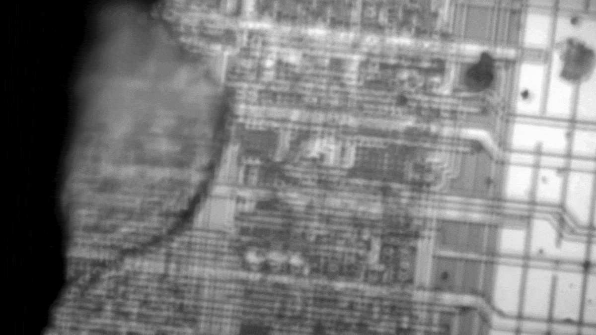
https://hackaday.io/project/179493-mobile-display-reverse-engineering
Before I scare everyone of with this long writing, please watch the short video I made about the machine basic functionality:
Story
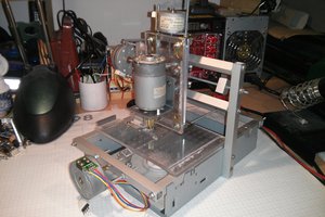
I mentioned I wanted a good microscope for myself, but after a lot of try and error I came to a conclusion without good optical components will never have any good result, so I built the reflective microscope. After that I was using it with manual Z axes (with only a screw) and an old plotter base, converted to X-Y stage. I have realised without a good base I will never able to use the microscope for any usefull thing. You quest it I designed one and built the machine base.
This is how you can start with a couple day / week long project and end up with 1-2 year saga.
I do not have to mention, without a good software this machine not capable of any result...
Design
I have used Bosch compatible 2020 and 2040 aluminium profiles for the frame, the reason because easy to work with them and at the end those with the right design can give rigidity. Rigidity is very important factor when we talk about microns, very small amount of vibration or deformation can cause the microscope to become unusable.
It is a bit ridiculous to talk about rigidity when I used 3D printing for almost everything expect the frame. I have used PLA which is fine, PETG or ABS could be a better choice, but I had experience with PLA so I choosed it. I still think with right design it shoud not matter to much.
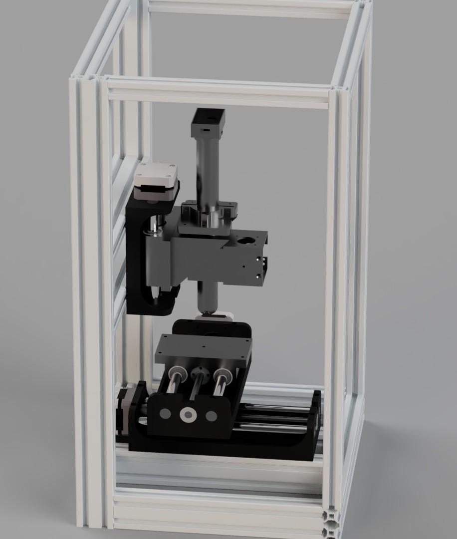
My main point about the axis setup was, I do not wanted to have a moving gantry. Also not wanted to mount the Z axes on top of the Y axes like usually moving gantry machine has. The reason is simly the further the microscope hang from the frame the higher the deformation and the vibration sensitivity.
The ideal type axis setup is Y axis is on top of the X axis and the microscope mounted only to the Z axes. This may not be the best option for every circumstance, but inmy case when the sample which I want to inspect is a few tens of grams maximum that will not cause deformation for sure. One down side for this setup is the frame have to be bigger than a gantry setup machine.
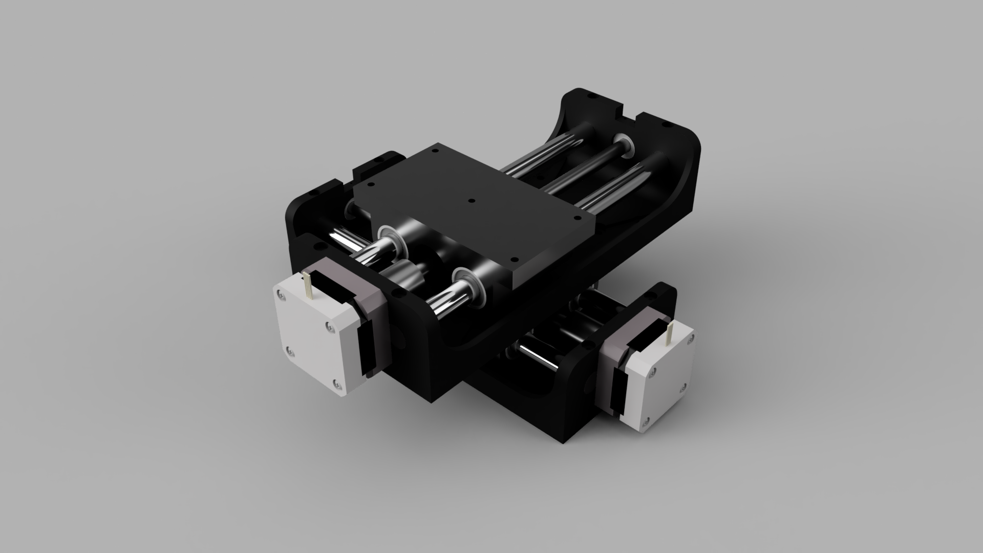
I have designed the axis only once and made it compatible to assambly an identical one perpendicular to it on top. The axis have a PLA base frame with 30% infill and two 12mm linear rod press fitted into it, this made the PLA frame quite rigid. For the motors I use some used 0.9 degree stepper motors with 8mm threaded trapezoidal rods (sadly I could not find local 2mm trepezoidal rods).
The carriage also printed in PLA and press fitted the 12mm long linear bearings. Made place for the anti-backlash nuts which are cheap chineese one, it is hard to call them anti-backlash when it manufactured so cheap it has +-100micron backlash...
The Z axis design is the same just shortened.
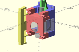
On the below two image you can see the X-Y axis and the whole machine rough design render:
The stage is also 3D printed, I have made it levelable with simmilar solution as 3D printers use for bed. There are 4 screws with springs ont he for corner of the stage and from up it can be leveled with allen key.
Building
I have...
Read more »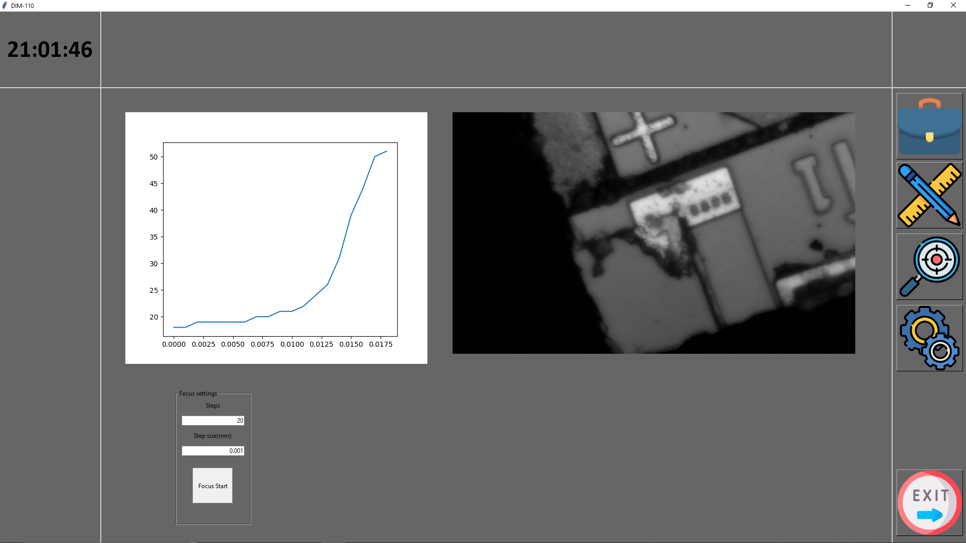


 rolmie
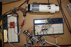
 Stefan Lochbrunner
 Kevin Kadooka