Lauri Pirttiaho
Novation Launchpads are a series of USB-MIDI controllers that are mainly used to control DAW SW. Using a Launchpad as a stand-alone MIDI controller requires changing the firmware and adding serial MIDI ports. This project is the initial reverse-engineering study of the HW to prepare for that.
This project is based on the original Novation Launchpad Mini which is sometimes detailed as mark1 (mk1), hereafter called nlp mini, which has been now superceded by newer version like mk2 and mk3.
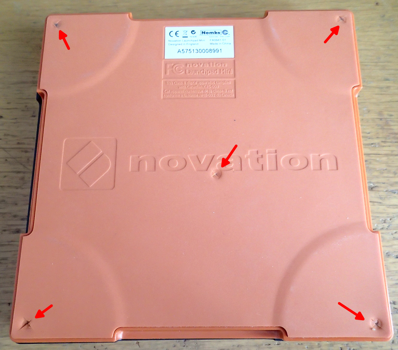
Nlp mini can be opened non-destructively by cutting the silicone pad glued to the bottom of the device. After the five screws have been removed, top and bottom can be separated by carefully disengaging the snap fits around the device. The board is clamped between the top and the bottom covers, not fastened in any other way.
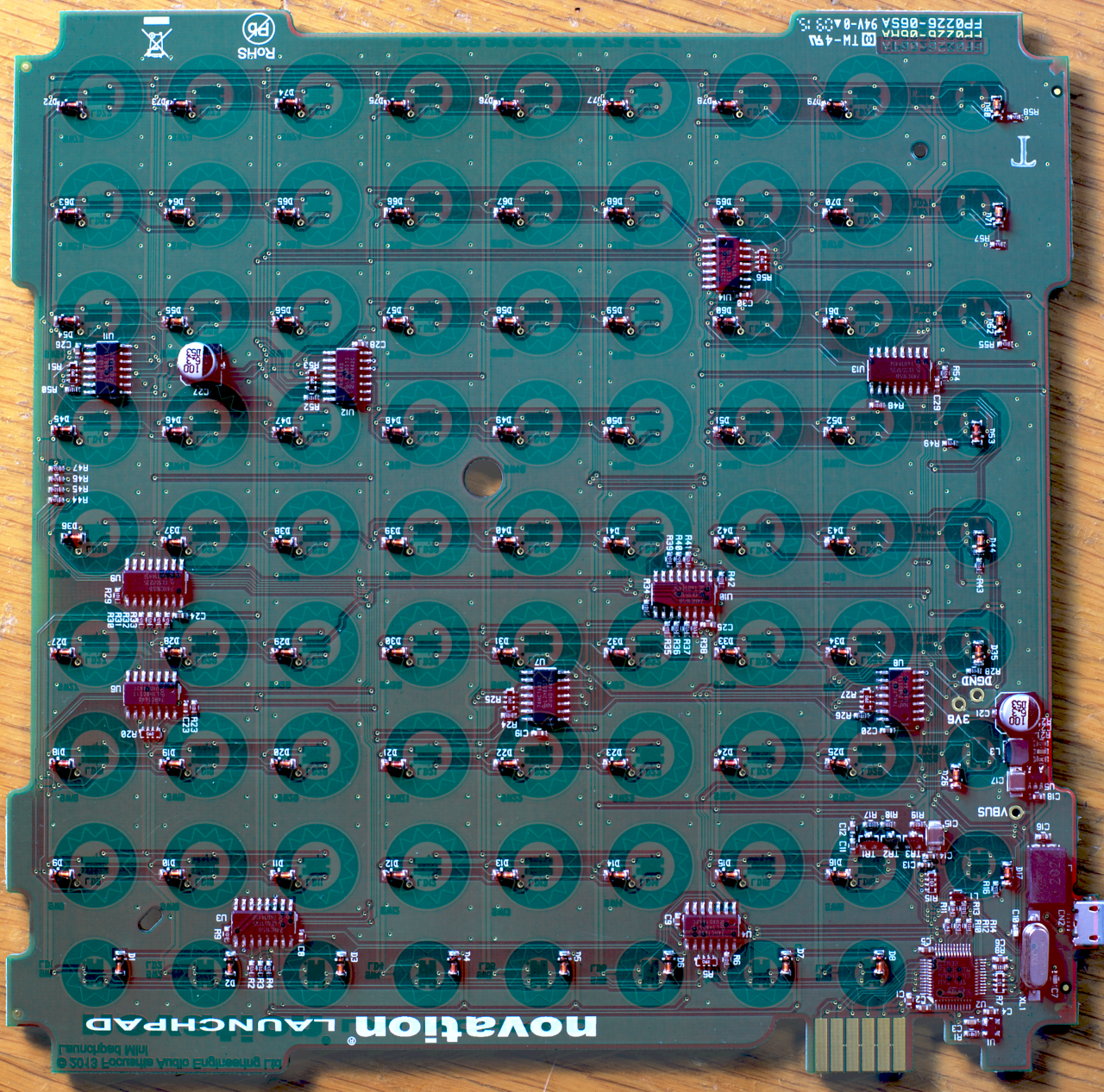
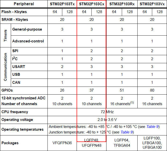
The microcontroller in nlp mini is STM32F103C8T6, 48-pin package with Cortex-M3, 64 kB of FLASH, 20 kB of RAM, FS USB (MIDI and vendor protocols), 2 SPI ports (one for switch input, other for LED control), 2 I2C ports (unused), 3 UARTs (unused) and plenty of timers. Of the 37 IO-pins the design uses 2 pins for the 6 MHz crystal oscillator, 5 pins for JTAG (full debug support), 3 pins for USB, 2 pins for SPI output to LED drivers, 3 pins for SPI button input and capture, and 3 pins for 1:3 multiplexer used for both LEDs and buttons. That leaves 19 pins free for further use. In particular this will allow, for example, adding 3 bi-directional MIDI ports (6 pins), an LCD display, and other new features.
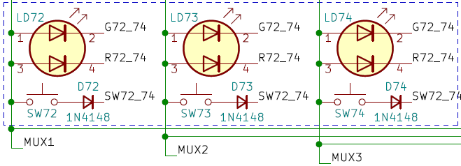
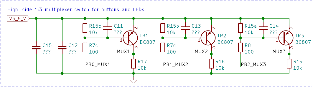
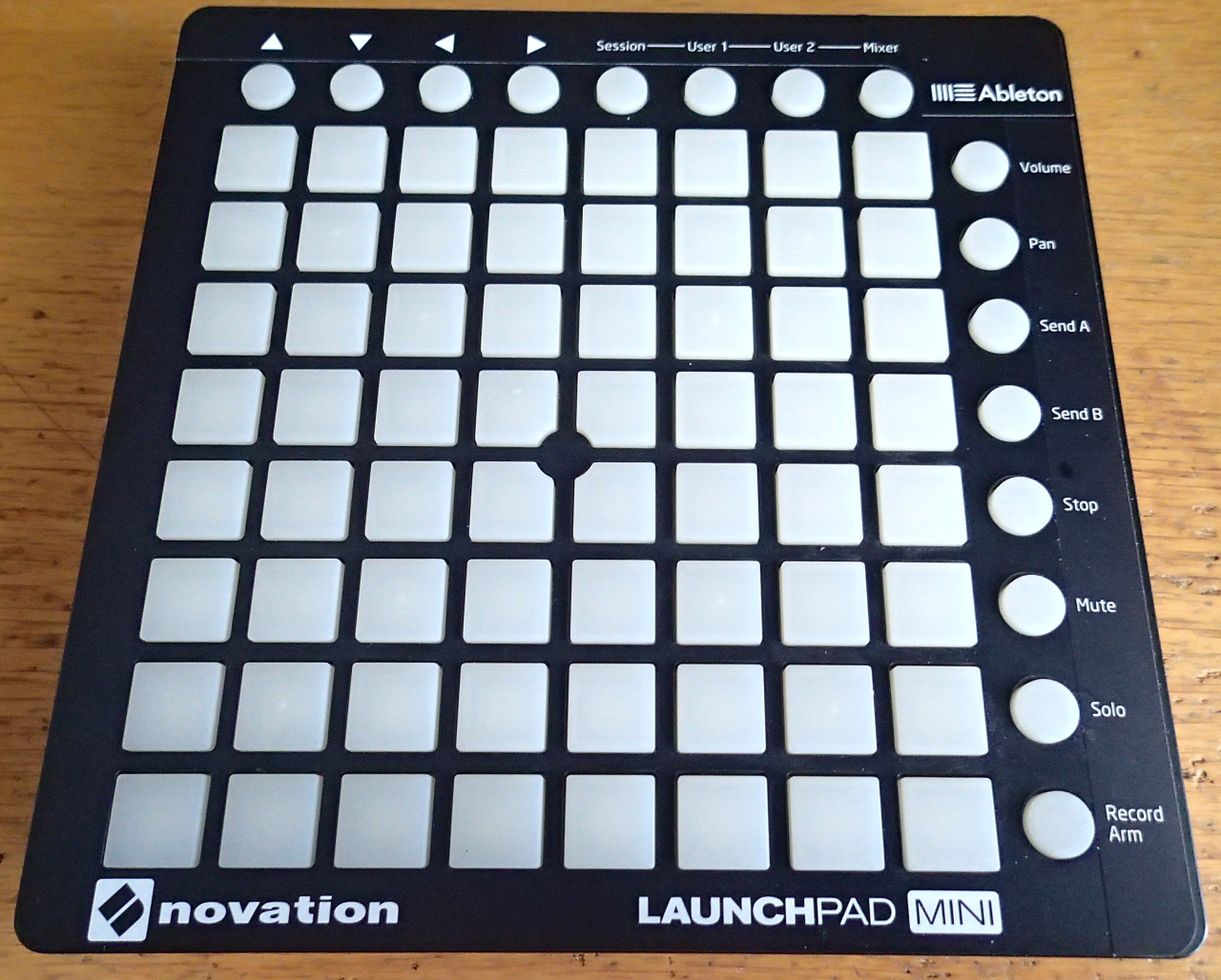
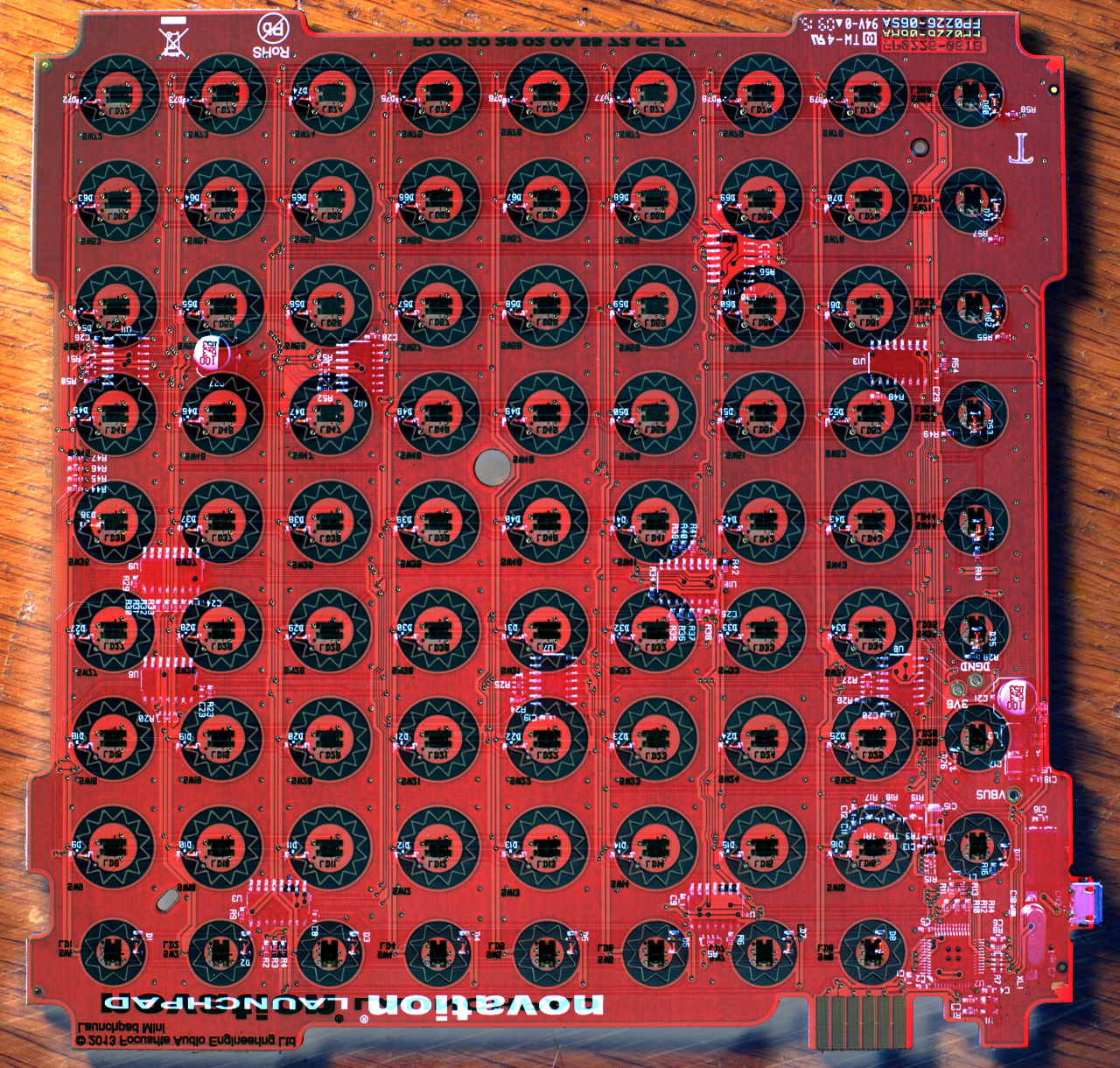
The control surface consists of 8x8 pad matrix and additional 8+8 pads aligned with pad rows and columns. Each unit consists of a rubber mat switch and a red-green bicolor LED. The units are driven from high-side with a three BC807-transistor switches in 1:3 multiplexing pattern. The LEDs are grounded using 74HC164 serial-to-parallel outputs with a red LED having 39Ω resistor in series and a green LED having none to balance the intensities. Each switch feeds through a 1N4148 diode to a grounded 47kΩ resistor connected from fed end to an input of a 74HC165 parallel load serial output converter.
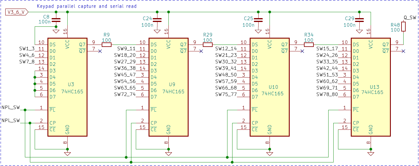
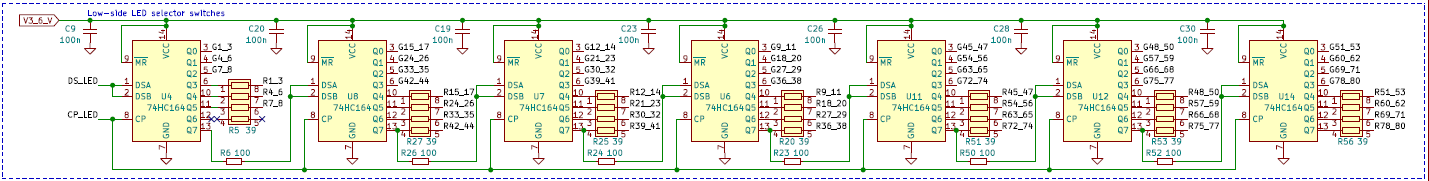
There are a total of seven 74HC164's and 4 four 74HC165's connected in chains and communicated using the two SPI ports. That would allow total of 3x7x8 = 168 LEDs of which 160 are in use and 3x4x8 = 96 switches of which 80 are in use. It might be possible to add 8 more LEDs and 16 switches to the system with small modifications to the HW.
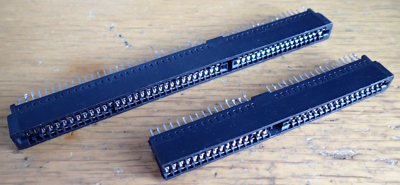
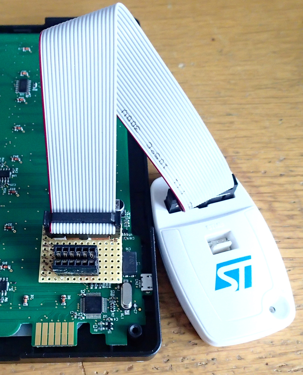
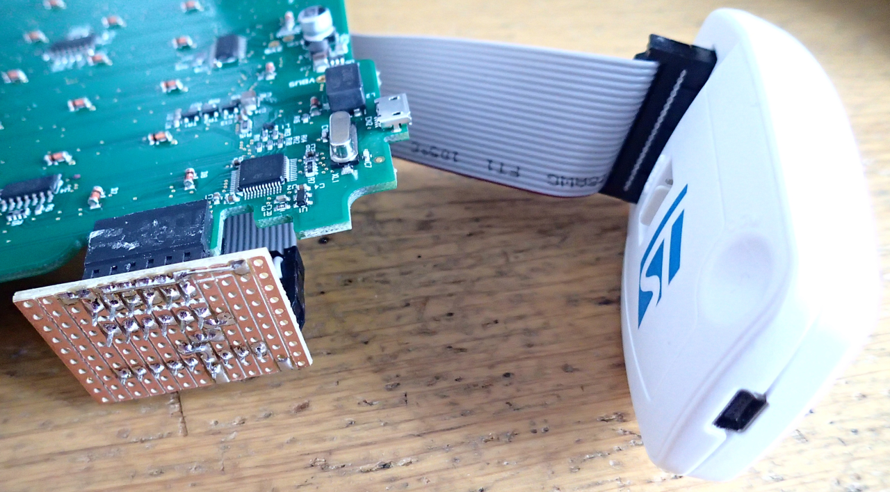
The JTAG connector on the PCB is somewhat uncommon, being a 2x6 pad board edge connector. The layout resembles the ST-LINK and J-Link pin orderings, so making an adapter for these is rather simple. Lacking a board edge slot connector, one can be easily crafted from an ISA slot salvaged from an old PC mother board.
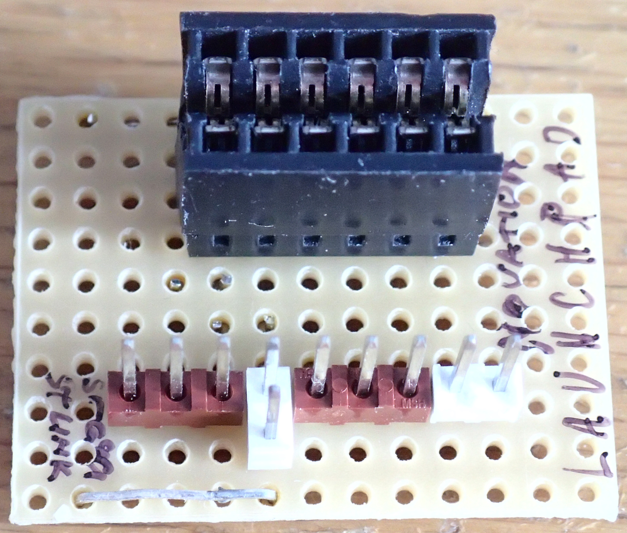
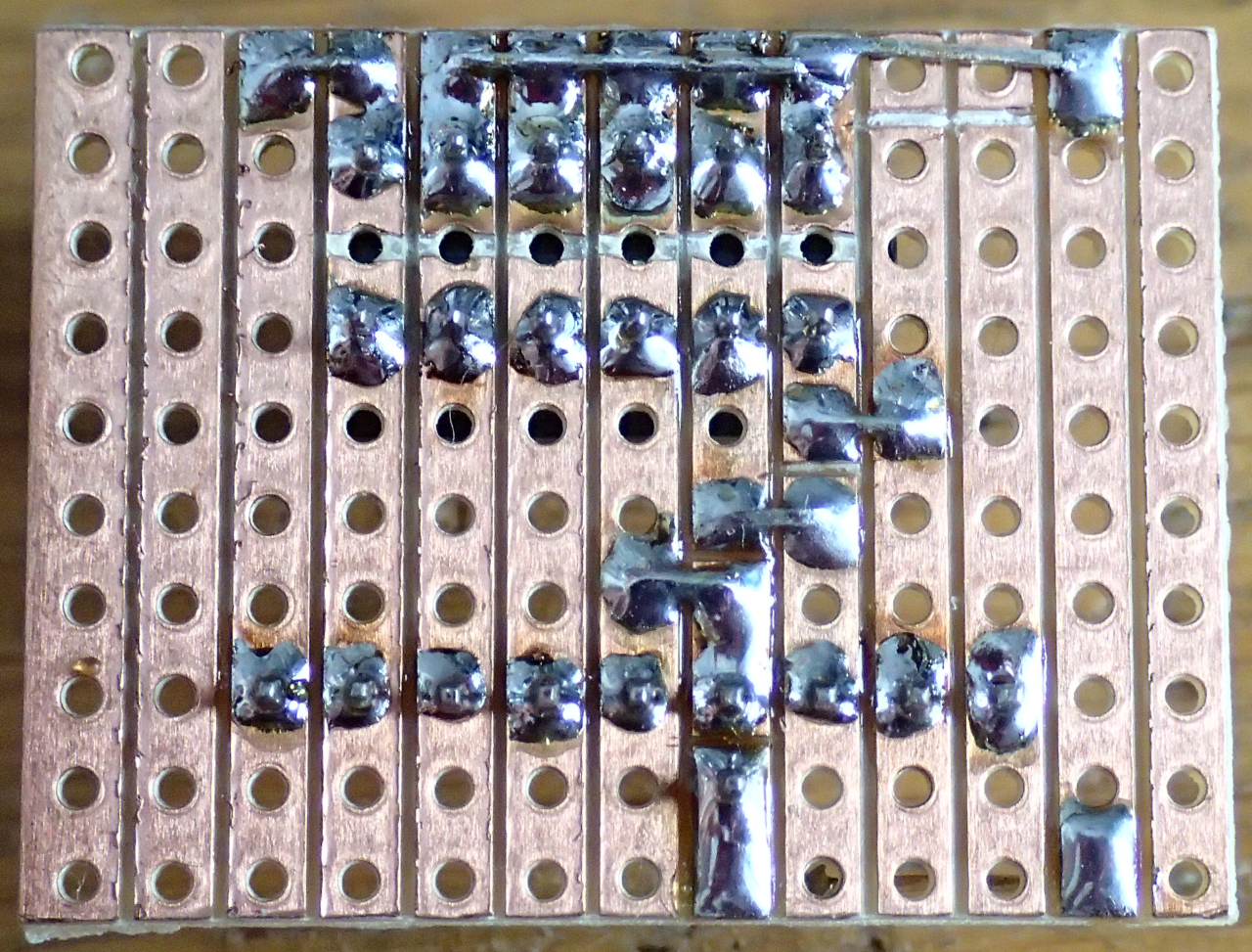
This adapter is for ST-LINK/V2.
 Just4Fun
 Sander van de Bor
 bornach