Lithium ION
When we go on large scale production of electronics modules, sensors and other Pcb circuits. We need some machines to do heavy tasks. But if the production is limited to some hundreds of Pieces, then assembling components took a lot of time. Unequal solder layer and hand soldering is too difficult in that case. Most of the circuits are using 0402 components these days to reduce the cost and surface area also. So we need a better method without investing in bigger machines.
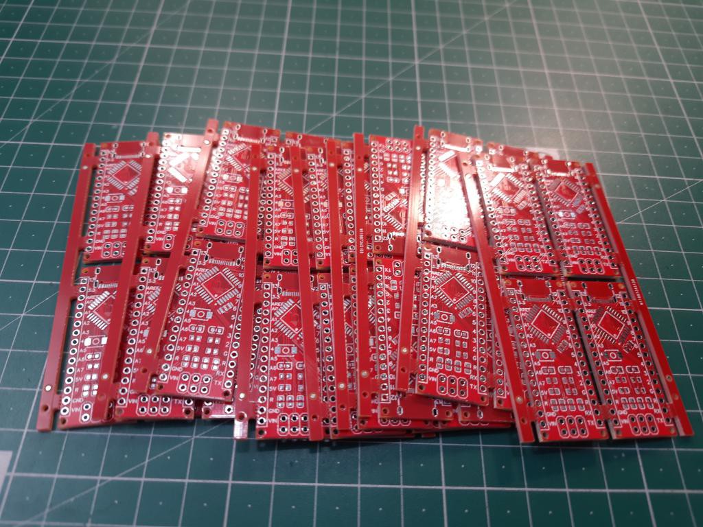
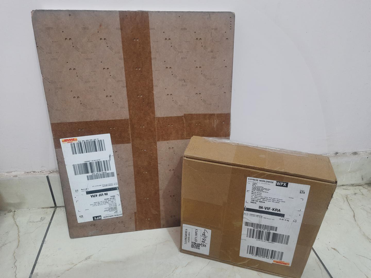
Then stencils come into play to distribute a constant layer of solder paste all over the PCB. But there are too many companies offering the service. I get may hands on PCBWAY stencil service. Because I am manufacturing my own microcontroller boards here in INDIA but on lower scale. My business is limited to school and college projects for now. So, I only need 40-50 boards per month.
Here I will show you how the stencil work and their importance in small scale business like my one.
Stencil:
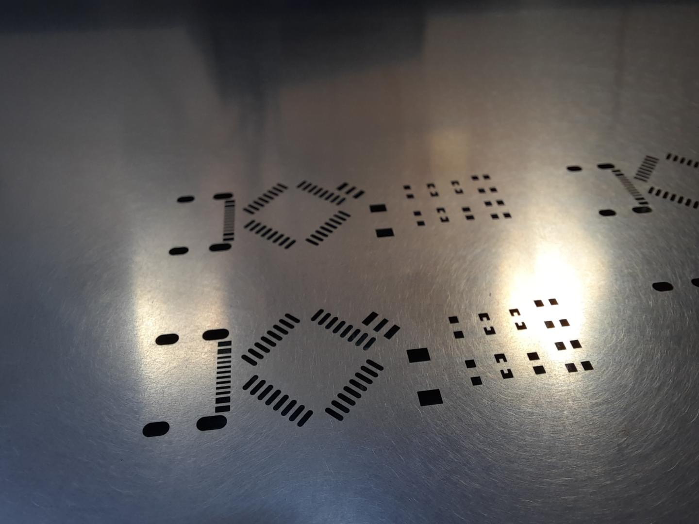
A PCB Stencil is a sheet of stainless steel with laser-cut openings used to place solder paste on a PCB board for surface mount component placement. The PCB stencil is used to deposit solder paste on designated places on a bare PCB board so that components can be placed and perfectly aligned on the board.
Nowadays, they are of two types. Framework stencils and non-framework stencils.
Framework/ Non-framework:
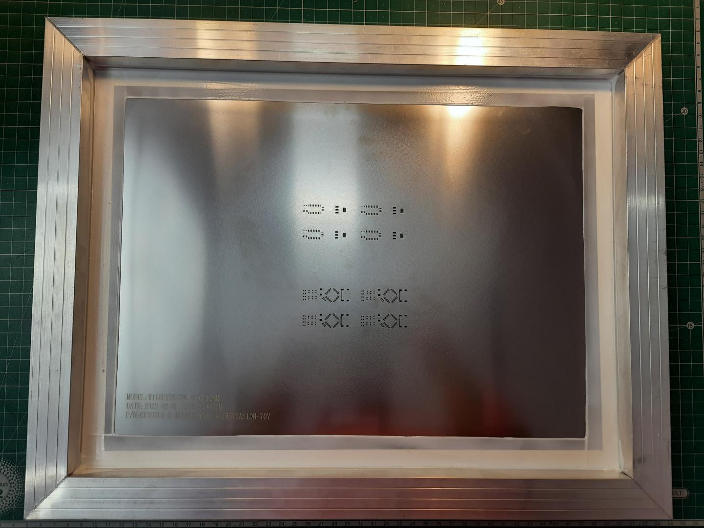
The framework is for automatic stencil machines and non-framework is for hand soldering. Usually, framework is heavier and bigger than non-framework stencil. Framework stencil have a rectangular aluminum frame so the cost of this one is obviously higher than other.
And I am here Because I am not aware of it, I do not have any stencil machine and I ordered framework stencil. So, to know more about the non-framework and the difference between the both you can visit PCBWAY official stencil guide.
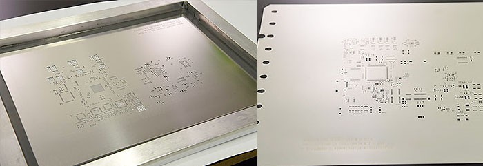
Framework stencil:
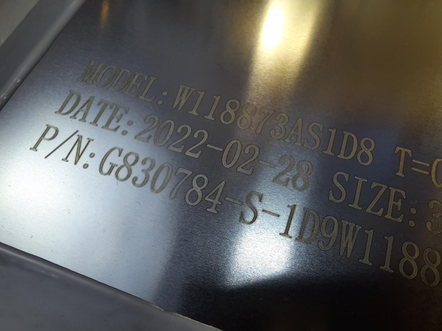
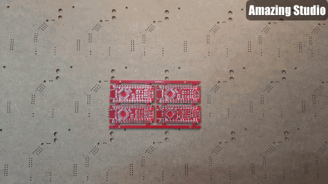
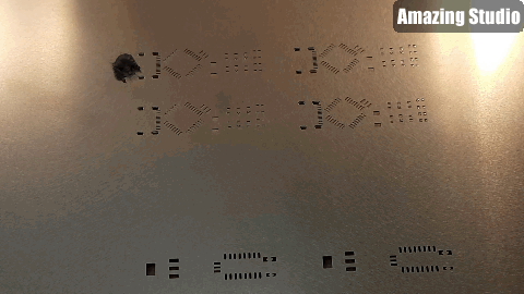
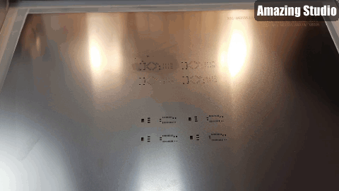
I was a bit scared when I received this beast on my location. It’s too big and heavy then expected. Here is a reference Image you can see and make an idea. I got very fine solder layer holes and frame is made of thick aluminum. Some order numbers or stock is drilled on one side.
I am using it for one design consisting top and bottom solder layer on one stencil.
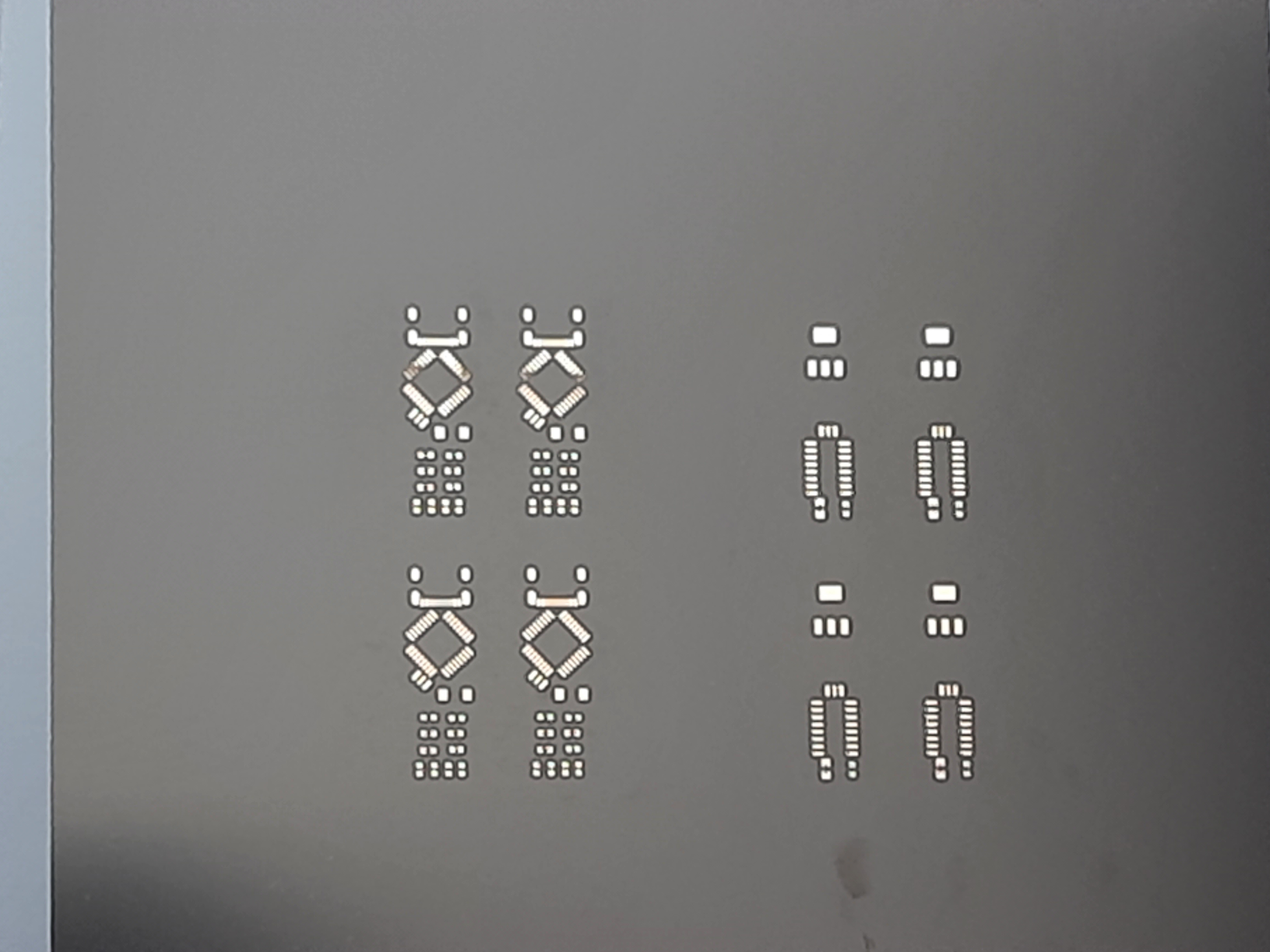
Top/bottom layer:
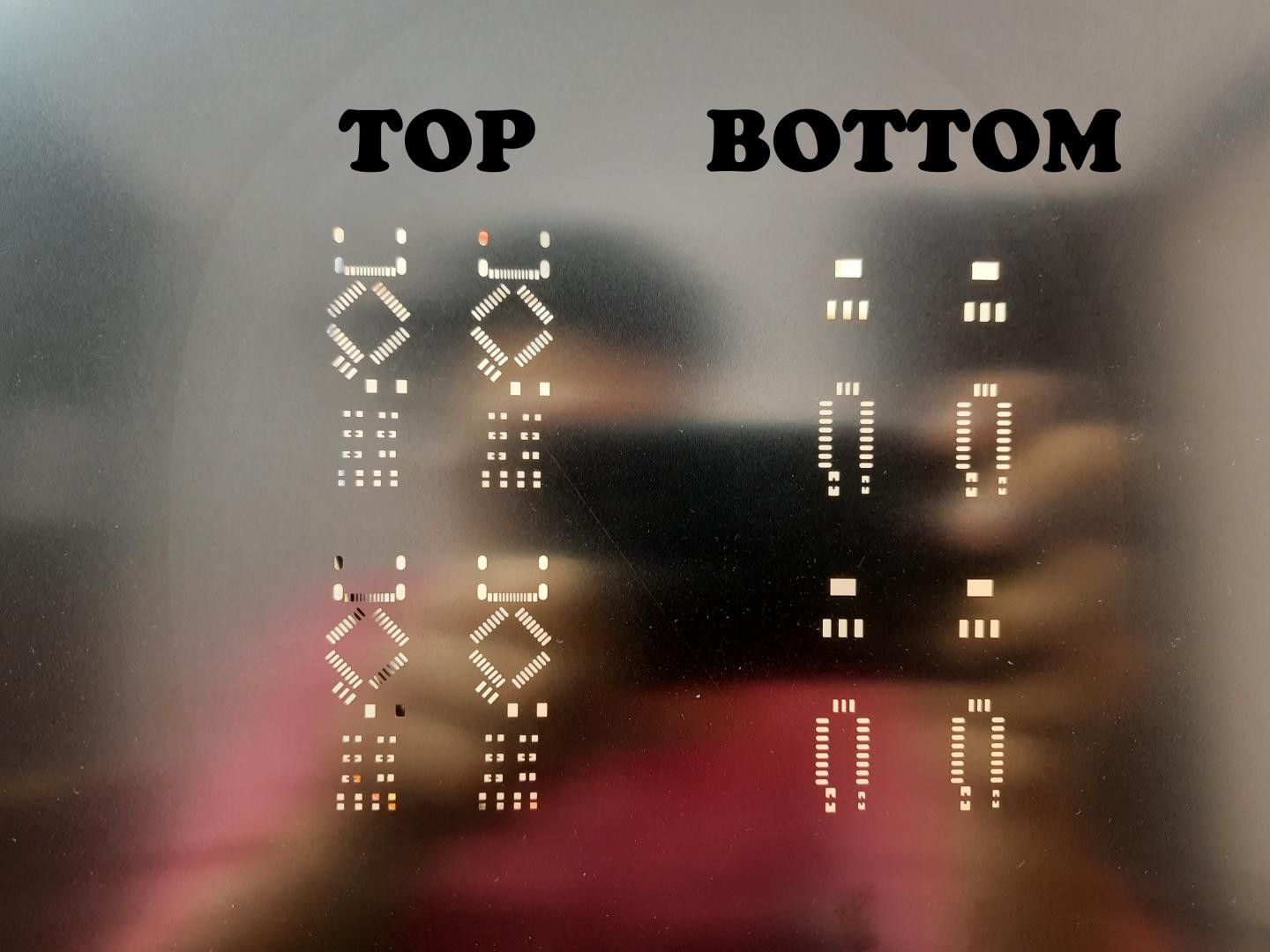
I am using it for one design consisting top and bottom solder layer on one single stencil. My PCB’s are Paneled as 2x2, here you can see one side is for bottom layer and other one is for top layer.
Using a stencil:
Because I have framework one, I adjusted my PCB on a MDF sheet provided by PCBWAY with stencil and then taped this tightly with the help of other PCBs available in my workshop.
Then I put the stencil on it, hold it tightly, pour and paste a thin layer of solder paste all over the board. You can use old credit card or pcb for this.
lift the stencil after applying solder paste, and then we are ready for assembly and soldering work.
More parameters:
Existing Fiducials:
Fiducials are positioning points for automated stencil machines. The diameter of the fiducials is usually 1mm. We offered three options: none, half lasered and lasered through. Half lasered is a sunk bump, lasered through is a through-hole. Half lasered is for automated stencil machines. Lasered through is for hand solder or semi-automated stencil machine. Please note that if you choose half lasered or lasered through, but there are no fiducials inside, we’ll ignore this option.
Electropolishing:
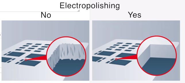
Electropolishing (also known as electrochemical deburring) will remove small burrs, improve the surface quality and provide smooth inside walls for better paste release. This treatment is mainly for IC lead width less than 0.5mm and BGA chips.
Ordering process:
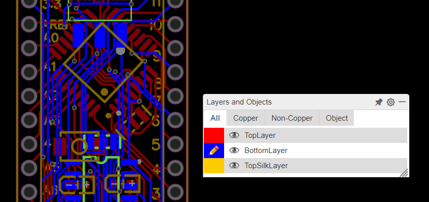
First of all you need to make Gerber files of Your PCB circuit. Gerber files made from softwares like Altium, eagle also have solder layer. In dual layer case it is named as top solder mask layer and bottom solder mask layer.
Stencil follow the cutouts according to the solder layer, there...
Read more »
 Jayken
 ElectroBoy
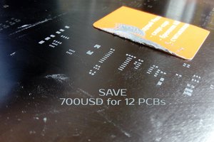
 Andrey V