 Anders Nielsen
This is another one of those things where I knew better, but still decided to leave it out of r0.
Thankfully I came to my senses and went for it: A semi-proper reset circuit. I had a close look at Garth Wilson's reset recommendations but decided against going all in with 555 timer monostables or DS1813's(wow those are expensive for what they do!)
Instead I went with Garth Wilson's design for NMOS 6502's but removed a pair of resistors and a diode to simplify things. As far as I can see the 1uF cap. and the first stage Schmitt-Trigger inverter is plenty of debouncing and a diode on the second inverter input seems superfluous as the input itself should already have protection diodes as part of the ESD protection.
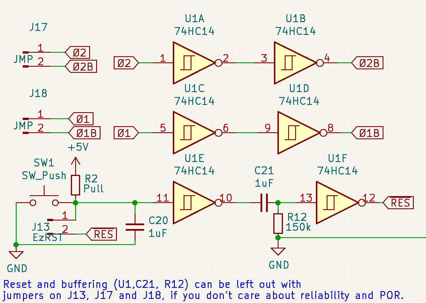
With regards to the clock buffering, I simply double invert phi2 and phi1. This is to prevent loading of the clock outputs of the 6502...
... but actually it's not even recommended to use the two clock outputs for anything at all. However since I had a lot more luck using them for my video bus sharing, than using just the 2Mhz input signal a.k.a. phi0, along with the inverted version, I decided to leave the circuit this way until that issue is resolved.
When testing R1 I was very happy I did it this way, since it lets you test new clocks without cutting traces and soldering jumper wires. By simply leaving out U1 and placing a jumper on the reset line J13(which falls back to a slightly debounced reset signal) it's easy to feed the two clock lines with a different signal - for instance phi0 + phi0 inverted.
As a side note I think the reason it doesn't work to just use phi0 and ~phi0 is two fold:
1) Phi2 is about 30-50ns delayed compared to phi0, but the 6502 operates(including data and address line timing) according to phi2. When using the data bus 100% of the time this is a problem when it's driven up to 50ns out of phase on one side.
2) Phi1 & phi2 are not 50% duty cycle - the high time of both are a little bit shorter than the low time, which decreases the issue of bus contention.
Worst case this means I have to make a phi0 derivative that's synced with phi2 and also has a shorter high than low time. For now this seems like too much work to fix a hypothetical issue, but I'm happy it's possible to test without hacking off pieces of the PCB.
That's about why I added this little part - and if you're short one 74HC14, you can still use the computer without it by adding the three jumpers.
Discussions
Become a Hackaday.io Member
Create an account to leave a comment. Already have an account? Log In.