 Christoph
The only low-capacitance probe I currently have is one of these FET Probes. And I had to have a look at the gate signal for a high-side FET in a BLDC motor controller. So why not try it with this one!
Here's the schematic for the gate driver and dual FET for one of this controller's motor phase outputs:
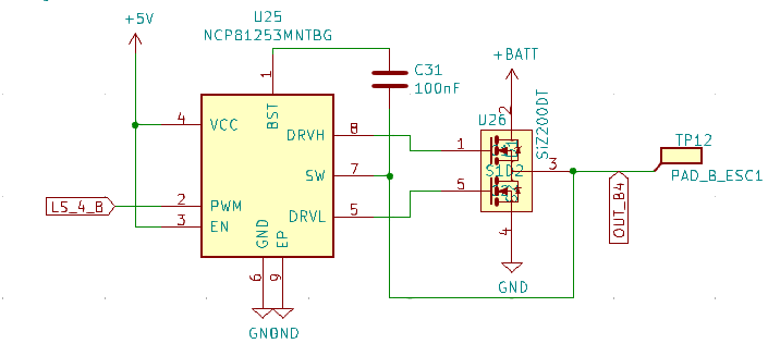
We want the gate signals to be clean: If they are too slow or wobbly, they might keep their FET in the linear range for longer than necessary, resulting in higher dissipation. The goal is a tidy step from "off" to "on".
While the motor phase is low, the gate driver can charge the bootstrap capacitor (C31 in the schematic) and then use the charge in that capacitor to switch the high side gate. When it's on, the motor phase will be at battery voltage and the capacitor floats above that. Any extra capacitance from probing will distort the signal, so we want to use a low capacitance probe like this FETProbe.
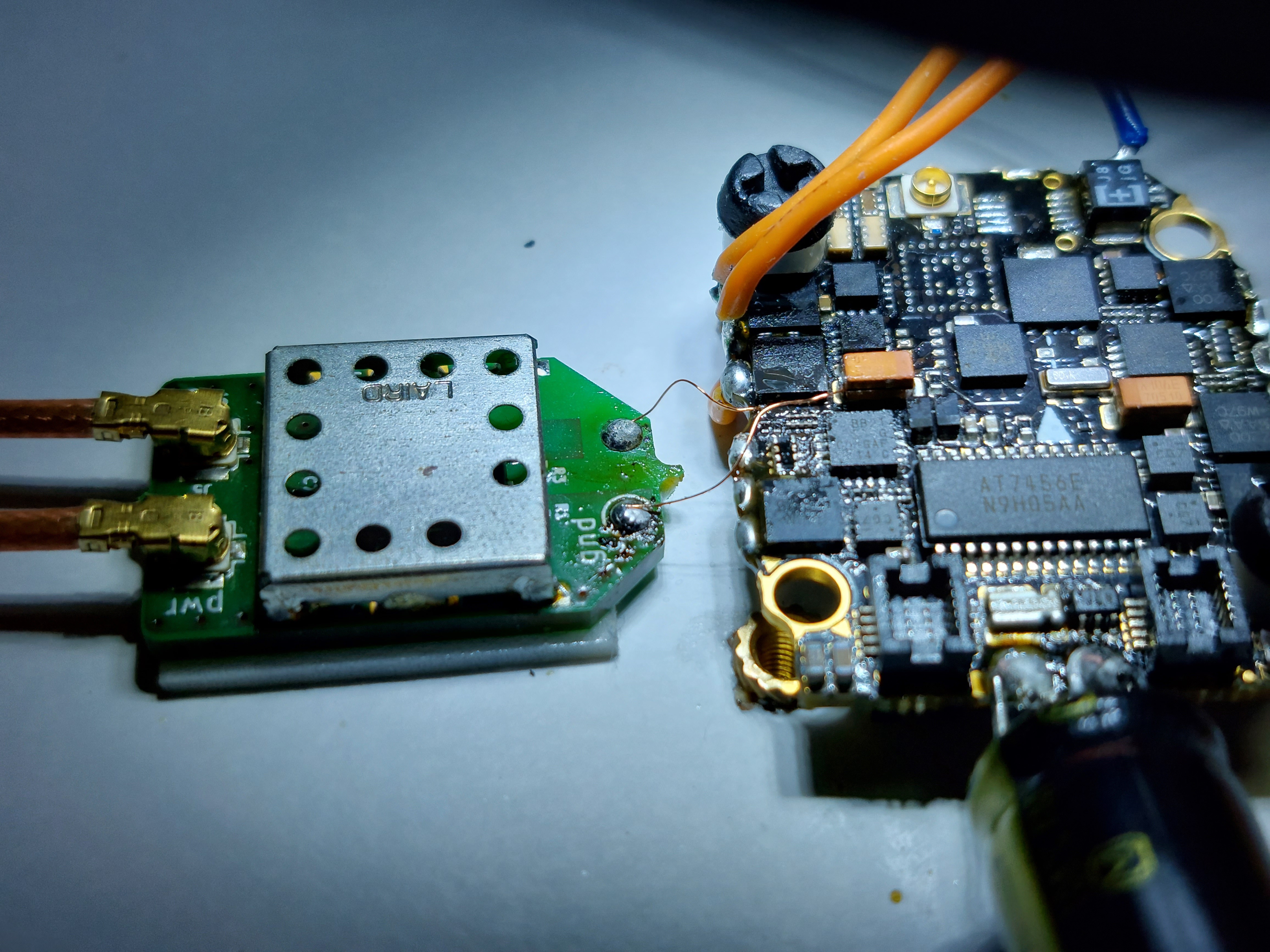
Soldering it into the device under test
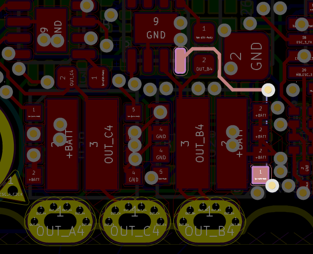
It's not that simple in this case, because the layout is pretty dense, but I found a good candidate which was even one of the longer gate signal traces in this design.
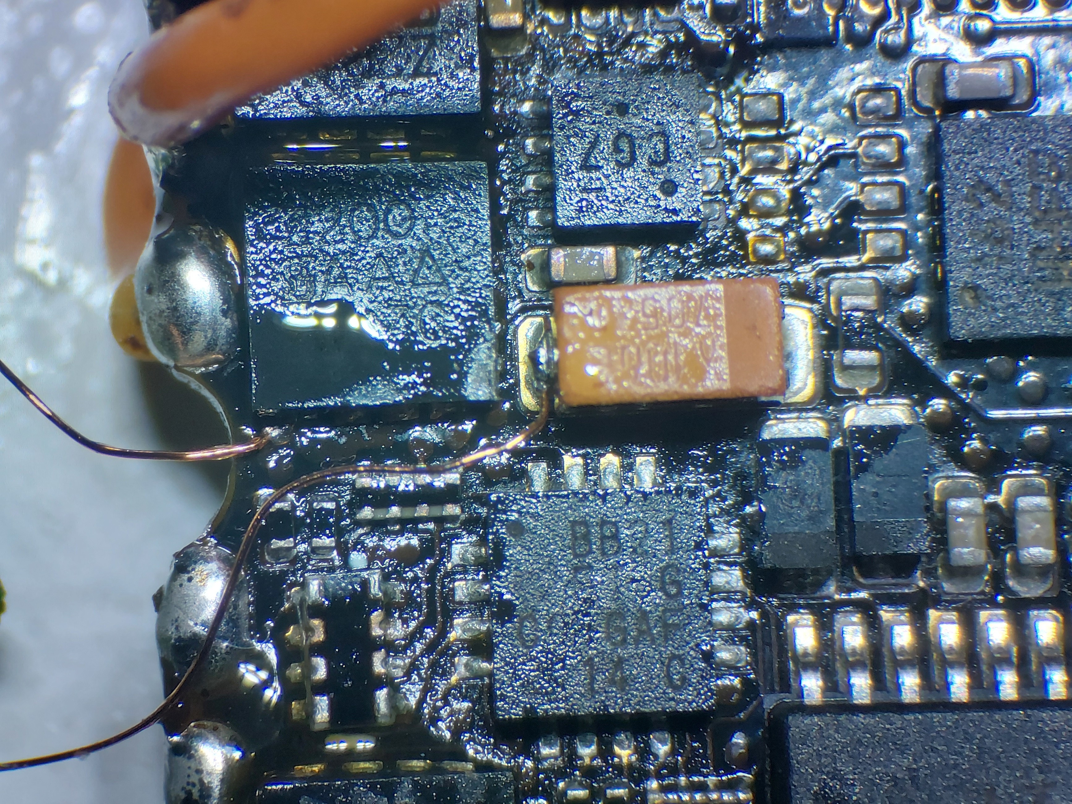
The gate signal layout:
With the probe attached, let's see what comes out of it. We have +BATT = 8V, so ideally the gate would float at 8 V and get switched to 13 V during the "on" time.
Here's a screenshot that shows the FETProbe's output AND that of a passive probe on the high side gate input:
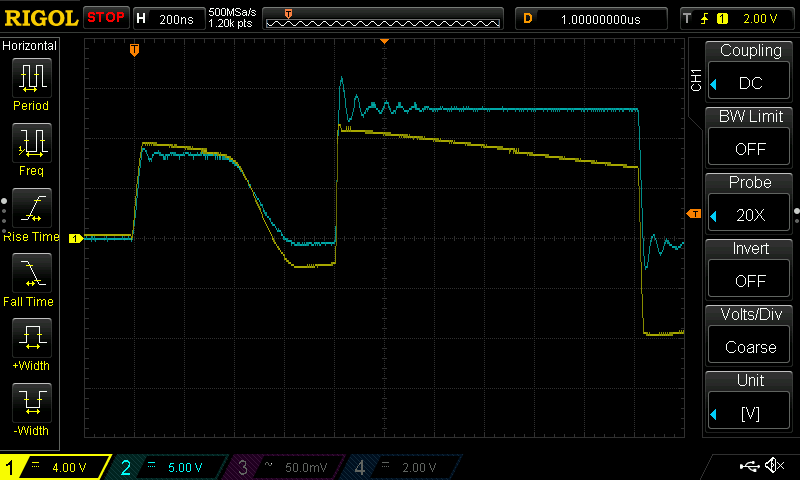
Ch1 (yellow): FETProbe
Ch2: passive probe for reference
In the first half we can see the controller's deadtime insertion. It's running bluejay firmware compiled for 40 deadtime units (roughly 800 ns, 4 horizontal divs). During this time, the phase is left floating and then drops to ground. After that, the high side FET is switch on and its gate jumps to around 8+5 V = 13 V. We can see that in the passive probe's output. However, the passive probe has high input capacitance and shows some wobbling. When we remove the passive probe, we get this from the FETProbe:
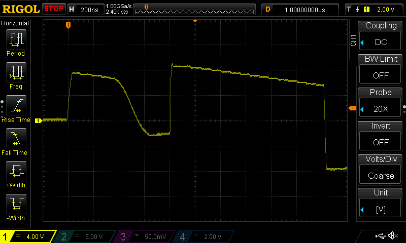
Looks pretty similar - really nothing to see here: the main takeaway is that the gate signal is pretty stable and clean. The ramps come from the FETProbe's AC coupling, and there's nothing we can do about this.
With the passive probe free, I decided to add the actual switching node to the scope screen:
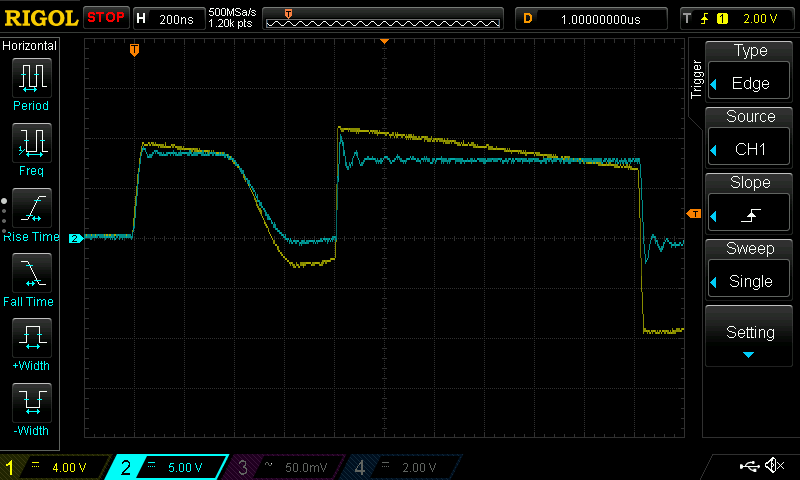
It's indeed switching between 0V and 8V, as expected, and the high side gate follows the switch node unless switched on.
Of course, DC coupled differential or single ended probes would be a better match for this task, but that's a different story.
Discussions
Become a Hackaday.io Member
Create an account to leave a comment. Already have an account? Log In.