ElectroBoy
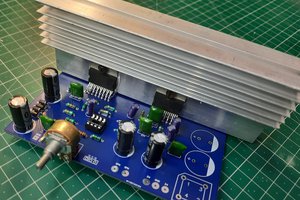
I made some simple amplifier board designs using TDA7294 IC, that one goes very popular among you guys. And today I am here to share the Preamplifier designs for 2.1 channel home theater and amplifier system. Here 2.1 refers to (2 speakers and 1 subwoofer). Because we are using Hi-Fi amplifiers which takes a lot of power, but the power is limited to half of the RMS without proper audio driver preamplifier stage.
Preamplifier need:
The basic fundaments of every amplifier are to produce maximum power, but again without high impedance at input and low impedance at output stage the power is limited to a few watts. And the stereo Bluetooth or Aux system can produce only 2 channels, Right and left which is consumed by Speakers then what about subwoofer.
Also, we need a low pass and high pass filter for the amplifier. So that low beats go to subwoofer and mid beats go to speaker channel. And if signal drops down then to re-boost the input by adding gain.
Now the needs are:
1) To provide one extra channel to drive subwoofer
2) Matching impedance according to amplifier input
3) Channel separator
4) Bass, Treble and Gain control
Components required:
1) JRC4558D
2) 1K, 10K, 15K, 680R, 100K, 150K resistor
3) 102j, 104j capacitor
4) IN4007 diodes
5) 220uf, 47uf capacitor
6) 100k, 47k potentiometer
7) 330ohm, 47k resistor
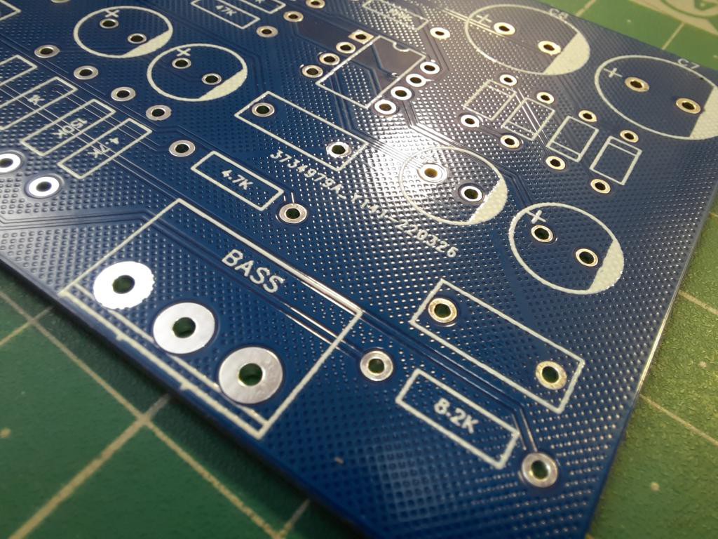
Circuit diagram:
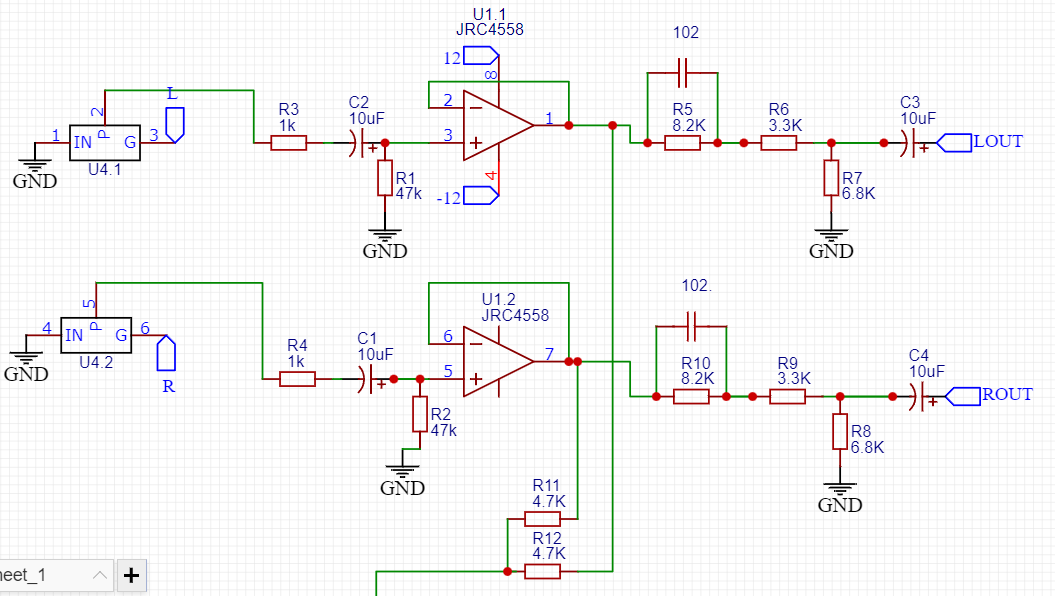
I designed the circuit in EasyEDA and here is my schematics, In the first section master volume control with speaker channels are adjusted using JRC 4558D operational amplifier as a gain controller and buffer. Then another channel is taken from the output of 1st operational amplifier and fed to the next.
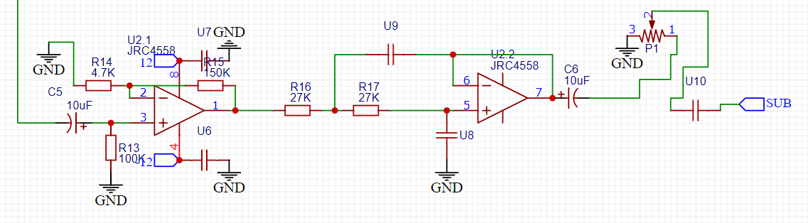
This time we are using operational amplifier as an integrator circuit which only passes the low frequency signals. Give a bass signal to drive the subwoofer, amplitude of the signal is controlled by 47k potentiometer.
PCB and Gerber files:
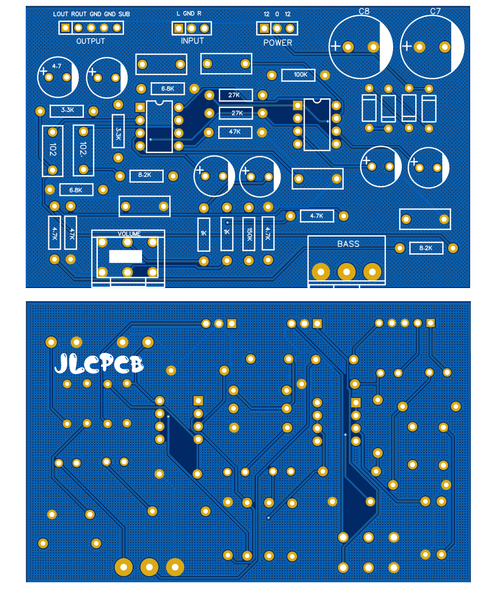
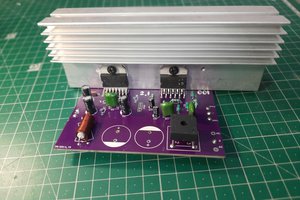
Then I adjusted all the components according to there connection properties and selecting line width to 0.4mm here is the final PCB.
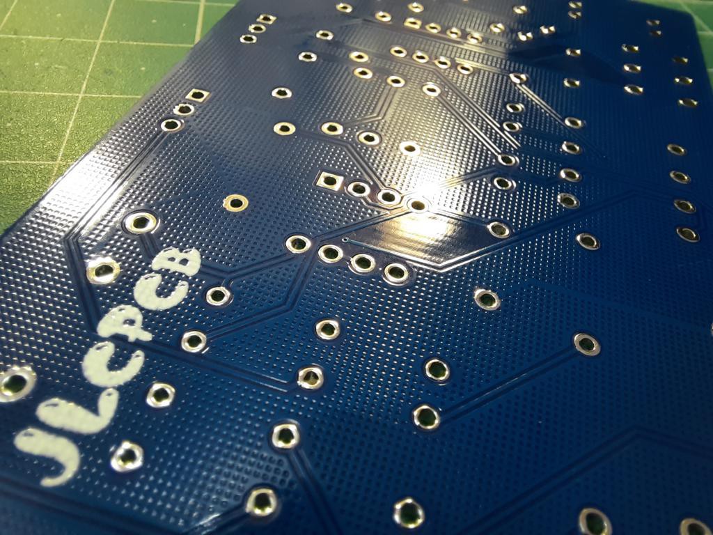
I am using blue color one, 1.2mm thickness and HASL with lead finish. PCB Is looking very gorgeous because of GND pad connection matrix. If you want to use same designs as mine then get them from here. JLCPCB is supporting my work here, they are providing 5pcs PCB just in $2. And if you sign-up using this link you will get free coupons of worth $30. Checkout JLCPCB from here and get your PCB just in 7 days.
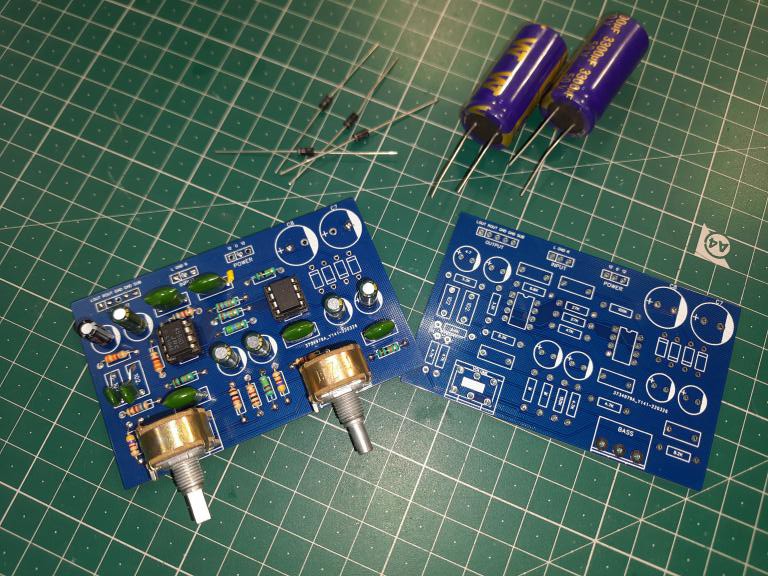
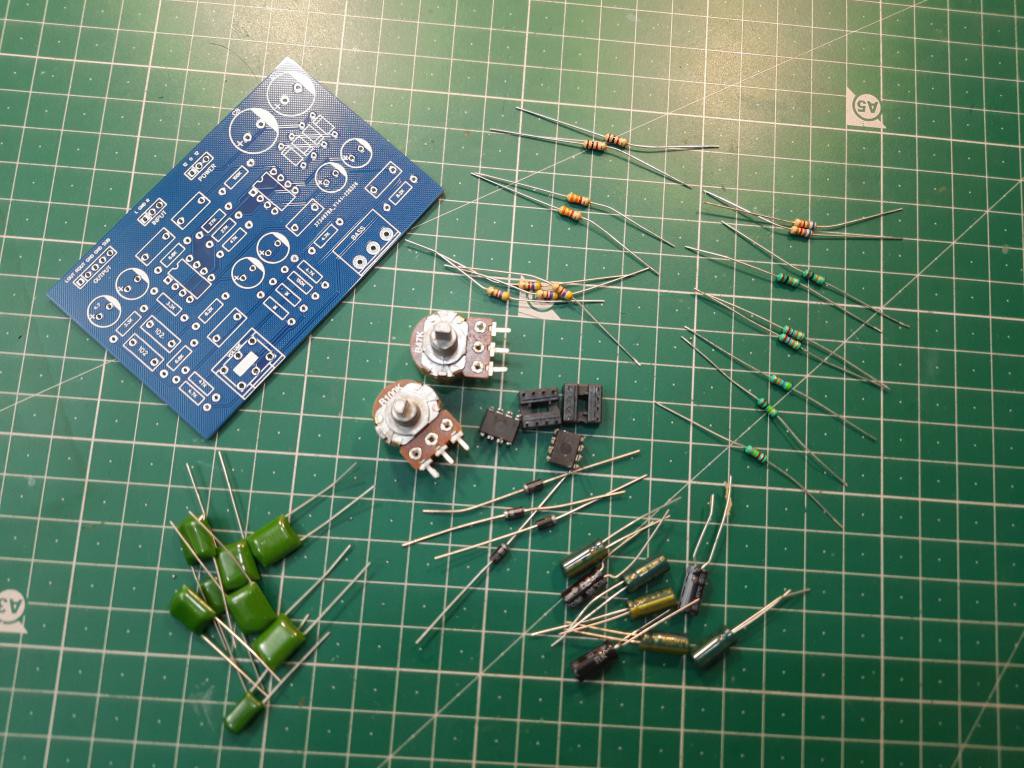
Assembling and Soldering:
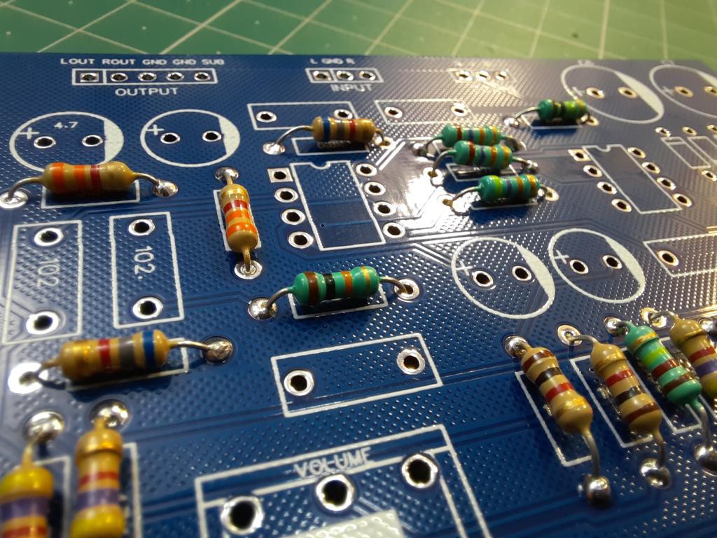
The best method to do the through hole assembly and soldering is, First place all the small components like resistors and diodes.
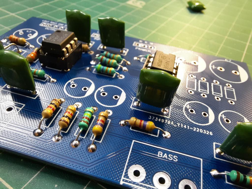
Then go with capacitors, ic and other required components. Ordering process is quite simple, just upload your Gerber files to JLCPCB choose thickness, finishing and color. Then checkout and receive your package in 7 days.
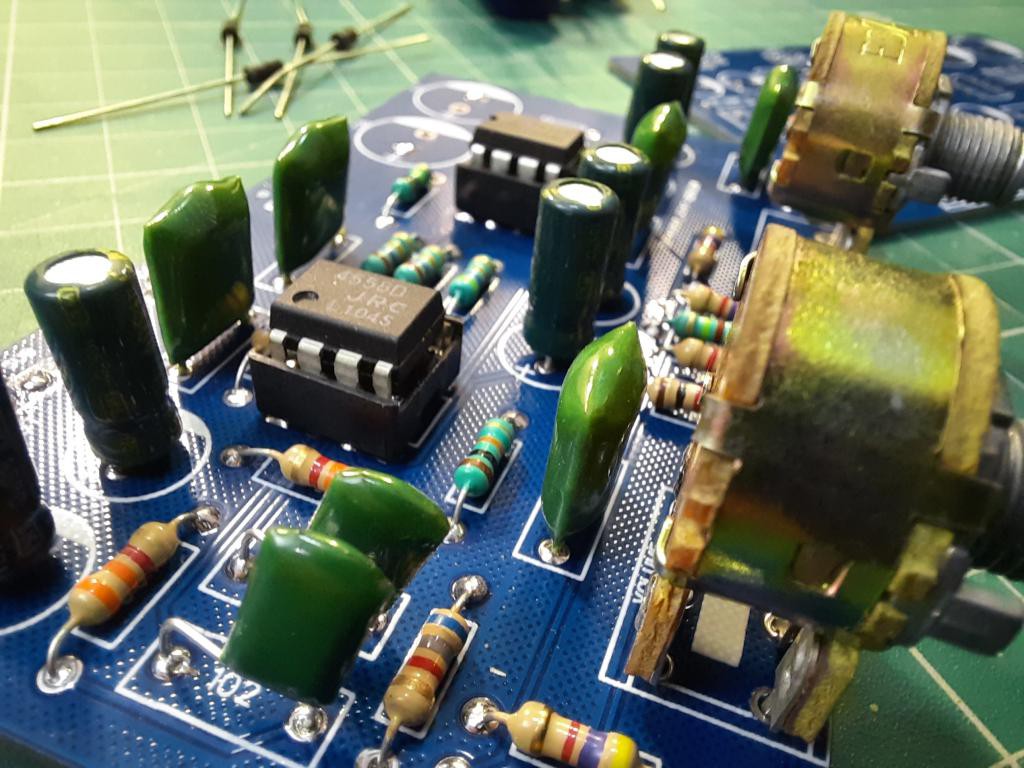
After this check the Circuit before mounting power supply section, this will give you better testing observations at different voltage levels.
Testing:
Power system:
Like the previous one this preamplifier also works in dual voltage of 12-0-12, You can put 4 diodes and 2 capacitor to complete the power section and then connect a center tapped transformer to it. Although circuit is taking only 100mA of current to produce a signal. A total of 300-500mA is sufficient for this preamplifier. Again big thanks to JLCPCB to give us this opportunity for working together.

 Lithium ION