ElectroBoy
Hello guys, last time I shared the circuit along with PCB layouts of 200w TDA7294 amplifier. You supported the article too much and now I am here to share a new schematic of 2.1 channel power amplifier. Here 2.1 channel refers to 2 speakers and 1 sub-woofer.
But we need a proper preamplifier to produce high and low beats separately. High frequency signal goes to speaker after amplify and low frequency bass signal goes to sub-woofer. So, we need a type of amplifier which can give stereo channel for amplifier and one extra channel for woofer. Which makes the circuit very perfect and give a pleasant effect too.

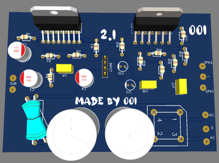
Then we will design our circuit on 2-layered PCB, because there are too many tracks and they can't be adjusted on single copper board. Here the JLCPCB prototype PCB service come to play, 5pcs of high quality boards just in $2. And if you sign-up using this link, you will get free coupons of worth $30 and other sign-up rewards. Checkout to JLCPCB right now for budget friendly and ultra quality PCB.
Circuit features:
1) It can produce stereo effect, Dolby enabled system.
2) Separate amplifier for Bass and High frequency signals.
3) Minimum noise and best output ever.
4) Onboard power supply and stable thermals
Components required:
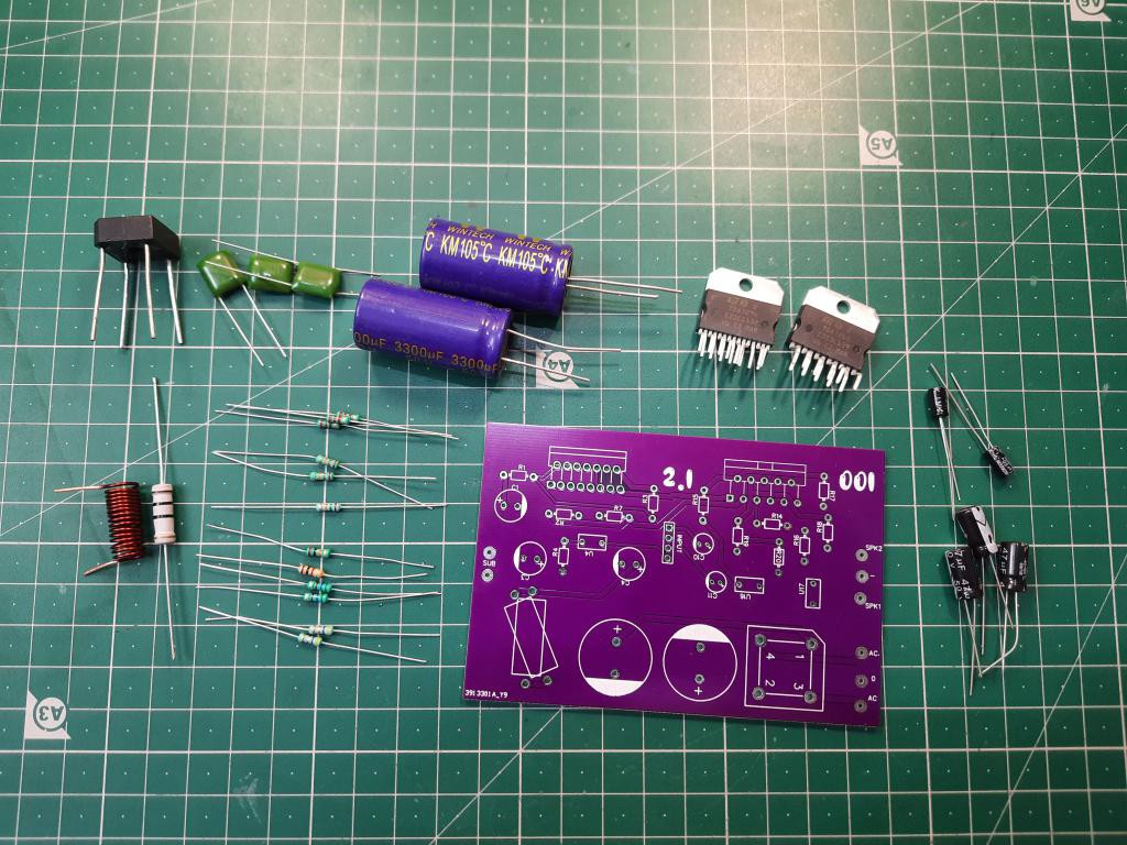
1) TDA7294
2) TDA7265
3) 22K, 1K, 18K, 15K, 560R, 4.7R resistors
4) 100nf capacitor (polyester)
5) 10nf capacitor (polyester)
6) 1uf, 47uf, 3300uf capacitor (electrolytic)
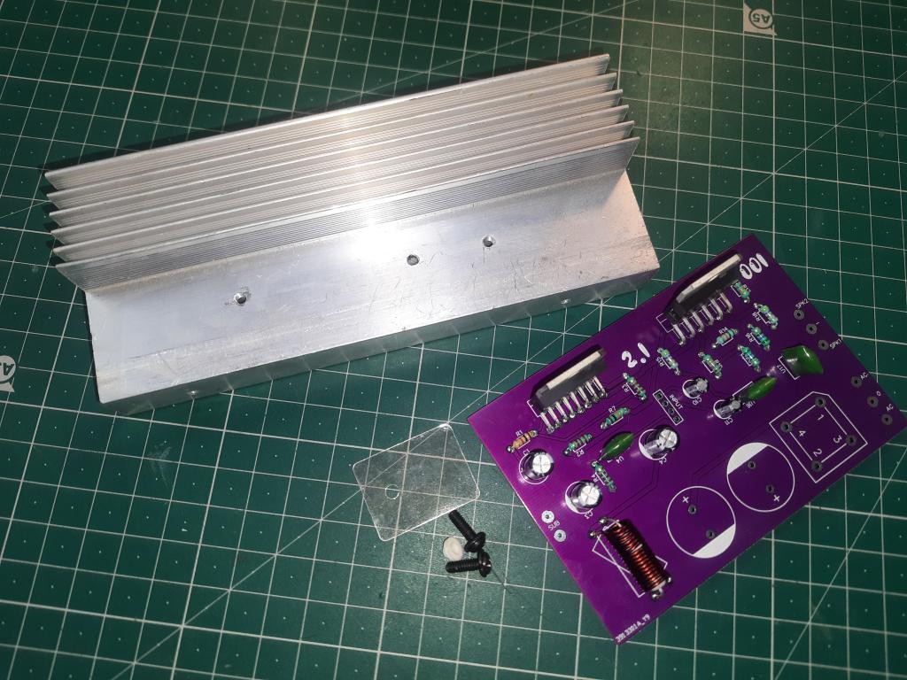
7) Big heatsink
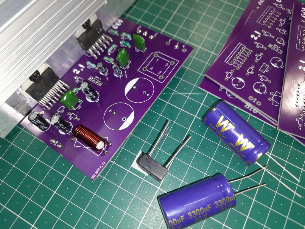
8) 6 ampere Rectifier brick
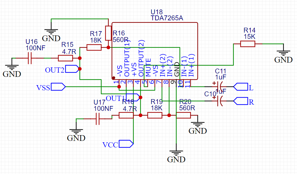
Use of TDA7294 and TDA7265:
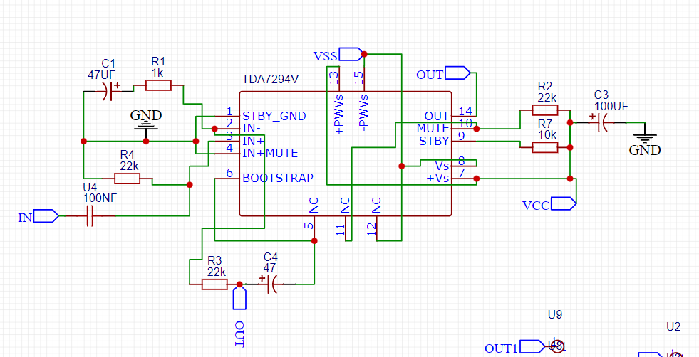
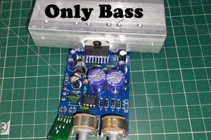
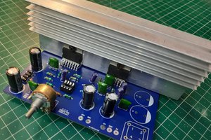
You can see two IC in the circuit, TDA 7294 can output 100watt RMS power and that is very enough for 8” subwoofer. But coming to the speakers, we need a separate low power dual channel amplifier IC. This work is done by TDA7265 ic which can supply 25w RMS per channel and support stereo output. So, a total output through the whole system is around 150watts.
For a home theater and car stereo system this is overpower. Because TDA series is known for High fidelity output and minimum noise. Power loss in heat is too much in these class AB amplifiers.
Circuit Diagram:
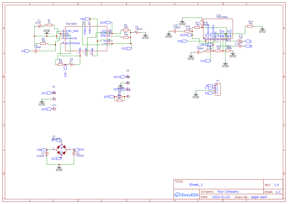
Here both the IC's use different configuration to produce sound. We are using TDA7294 in the project to take single channel 100w output but the output of TDA7265 is shared between two channels. A output of 50w is shared as 25+25 between both the speakers. Also for the power supply, A rectifier with filter capacitor is required. You can place the power section and then power-up the amplifier directly from transformer OR test before assembling the supply section using previous homemade filter supply.
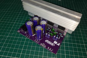
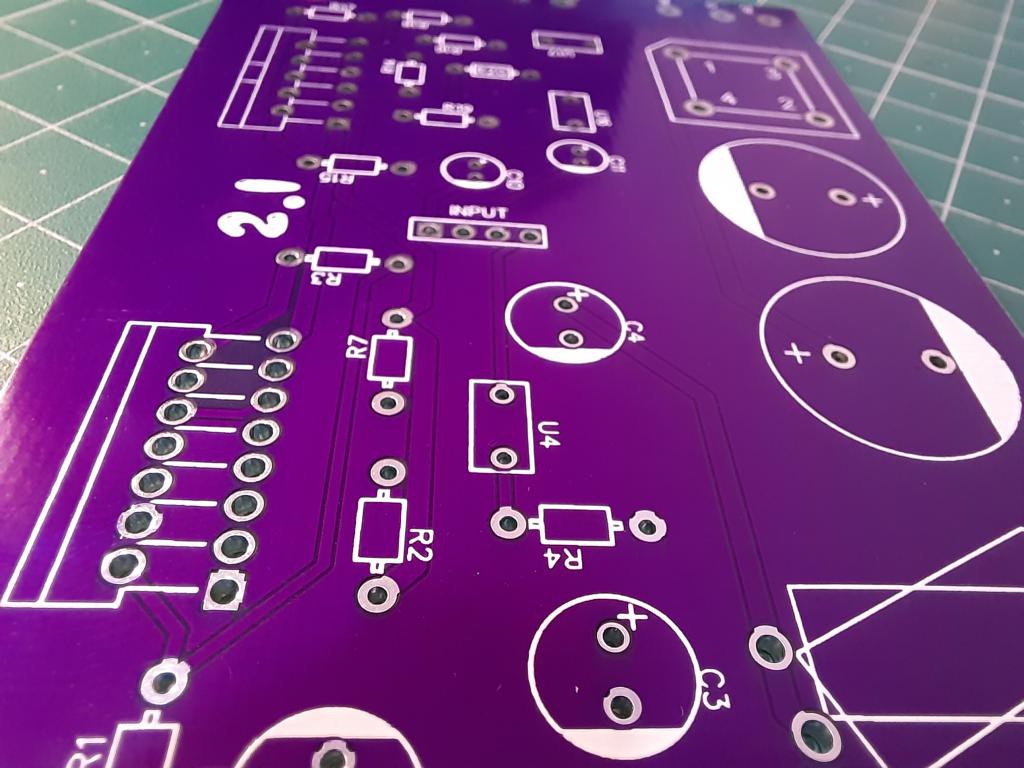
PCB layouts:
I designed the PCB from layout in EasyEDA, Keeping a lot of things like heatsink availability, holes, arrangement of components and thickness of tracks. This is the final PCB design. Yet, I have to do some modification in future regarding filteration.
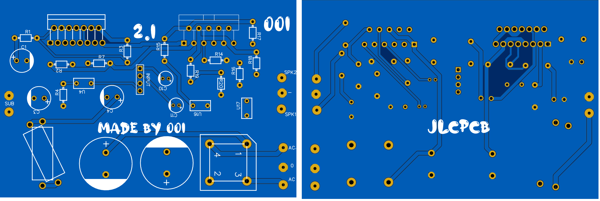
JLCPCB is the best PCB prototype service provider and you will get those beautiful designs just in $2. I am using 1.6mm thickness, purple solder mask and HASL with Lead finishing. By the way, if you want to use same designs as mine then Download Gerber files from here.
Soldering and assembling:
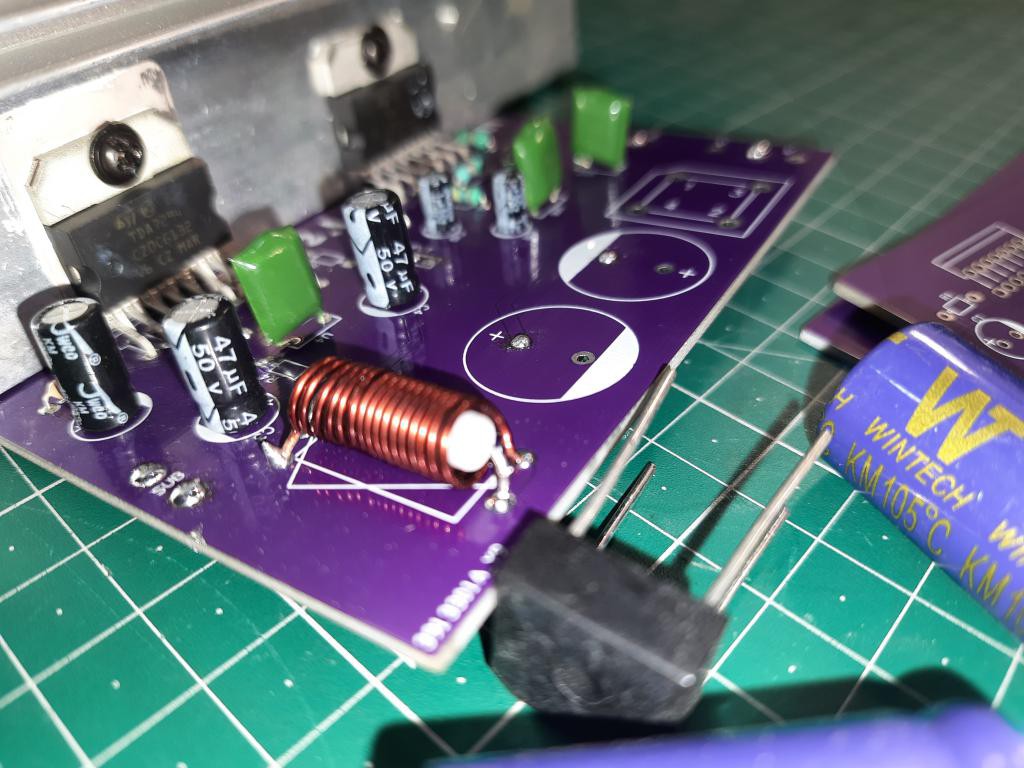
First of all solder all the small components like resistor and diodes. This will help to assemble your circuit fast and accurate.
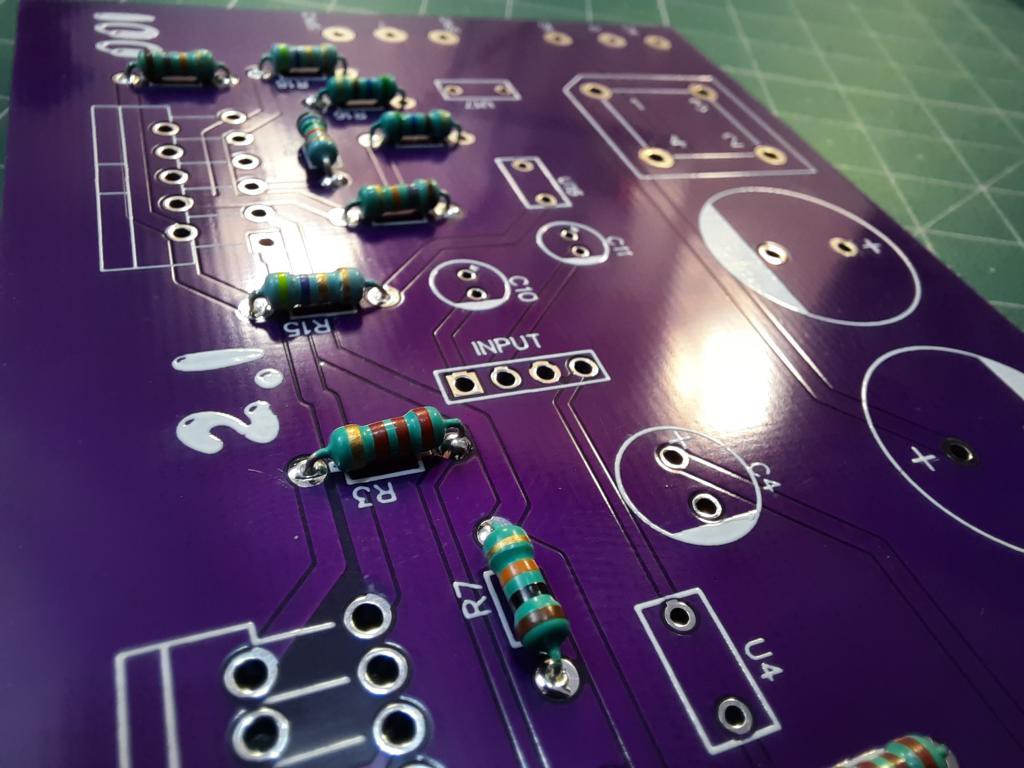
Then go for Capacitors, IC and other components.
Don't assemble power supply section if you already have dual filter power supply, this will help to measure the voltage to signal value by adjusting the volume.
Heatsink and thermals:
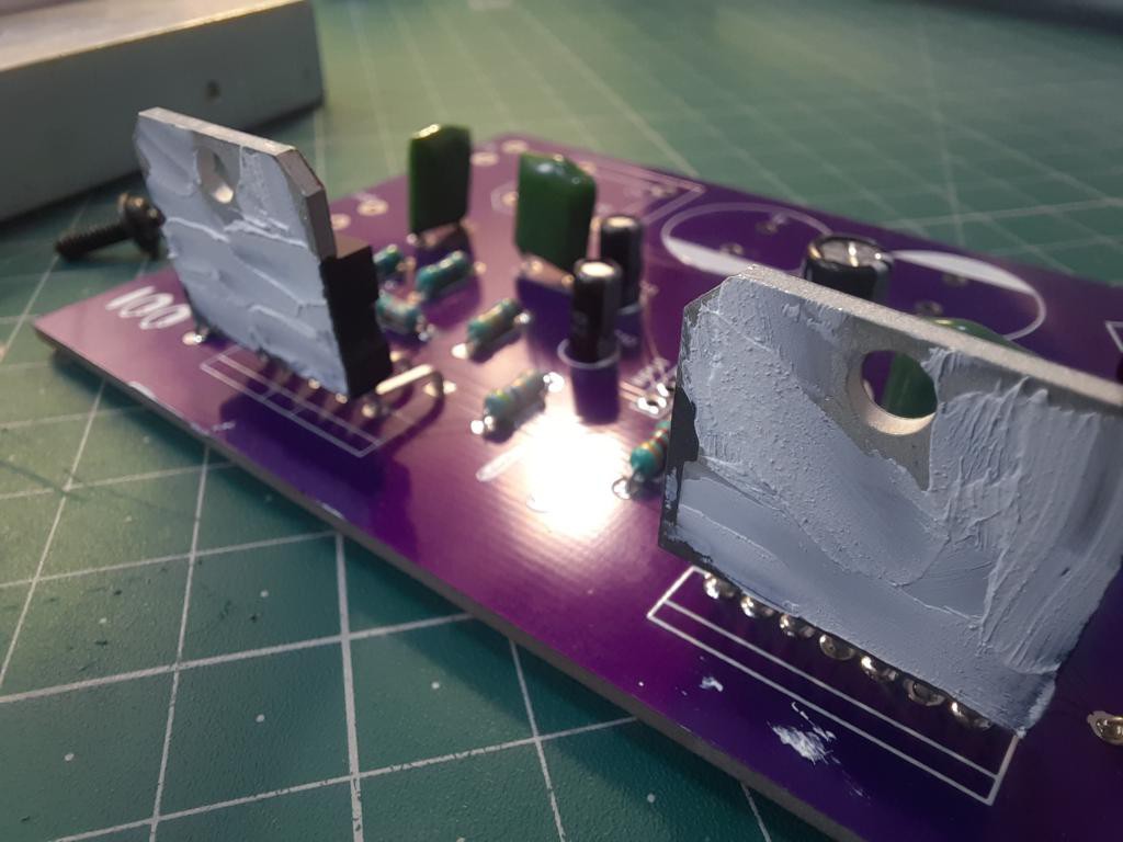
Because both the amplifier Ic's are of Class AB type, they generate a lot of heat. Without heatsink the design is not possible, it will automatically shut down by thermal protection.
So, we need a good big heatsink with proper heatsink compound to manage the thermals. Also cover one ic with mica sheet so that it will not make contact with other one, otherwise there will be a short circuit.
Testing:
This is the small video...
Read more »
 Sagar 001