 peter jansen
A quick update with a new sensor I've been working on, a magnetic imager tile (something like a "magnetic camera"). It's definitely very cool to see magnetic fields live!
Magnetic Imager Tile
I've always been interested in visualizing things that are challenging to visualize, particularly those that are pervasively around us. Magnetic fields certainly qualify for this -- I think it's absolutely fascinating that they're everywhere, but that we (generally) don't make more than point measurements of the fields, and only very rarely are images taken.
The most intuitive way to make an imager for something is to get a whole bunch of single sensors for that something, and place them in an array. Alternatively, you can take a single sensor, and physically translate it through space, as in Ted Yapo's magnetic field scanner ( https://hackaday.io/project/11865-3d-magnetic-field-scanner ). A few years ago I worked to build an imager by putting together an 8x8 array of the popular HMC5883L magnetometers, spaced about 1cm apart ( https://hackaday.io/project/5030-low-field-mri/log/15914-concept ). This has plenty of positives -- each sensor is a 3-axis magnetometer, and the whole array could be read using a simple I2C interface. Some of the difficulties are that such a large board with very tight-pitched components is a bit challenging to assemble -- I was only able to successfully assemble a 4x4 version, with the 8x8 (and it's 64 magnetometers) unfortunately only working as an object d'art. One of the other challenges with the HMC5883 array was the packing density -- the number of external components meant the maximum density I could achieve were pixels (magnetometers) spaced 10mm (1cm) apart.
It's been a few years since I had a go at this, and so I decided to put together another attempt:
- Simpler sensors: Large-pitch analog hall-effect sensors instead of I2C sensors.
- Higher density: a 4mm density using SOT-23 sensors requiring no external components
- Addressable array: Analog addressing through a large array of analog multiplexers on the back of the board
- Tileable: Able to create larger arrays by putting multiple boards adjacent to each other
- Easy to solder: Only large pitched components, so it would be quick and easy to solder in a toaster reflow oven (for the array side) and with a hand iron (for the analog multiplexer side)
- 12x12: The size of the array (12x12) makes it big enough to see interesting things, and small enough to (I hope) fit on the back of the eventual Iteration 8.
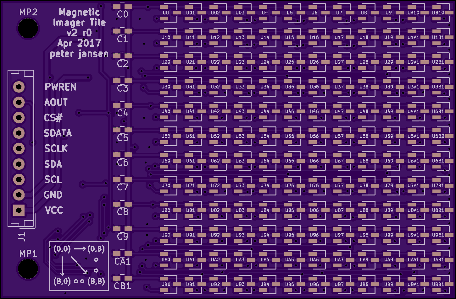
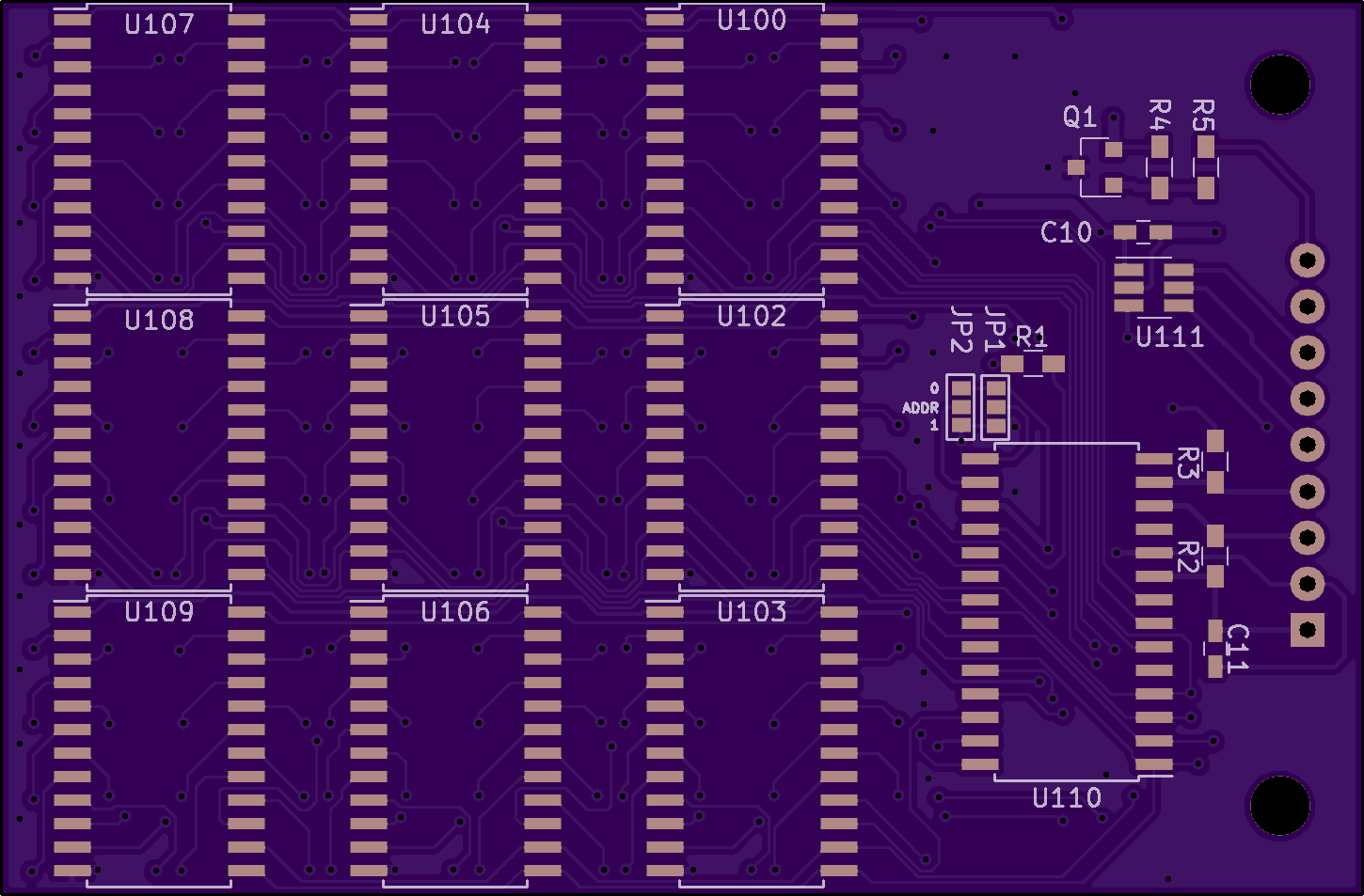
I learned from my earlier attempt with the HMC5883L array that this would be a bit of a routing nightmare, and so I decided to try switching from EagleCAD to the open source KiCAD, to make use of it's push-and-shove router. It took a bit of getting used to -- KiCAD still has significant usability issues, in my opinion -- but with some work the board artwork came together, with exactly enough room for everything. The Hall Effect sensors and power traces are on the top side of the board, with the array of analog multiplexers to route the analog signals from the sensors placed on the bottom. The bottom also contains an I2C I/O expander (U110) so that the array can be addressed using only 2 I2C pins instead of over a dozen address lines, as well as an external 14-bit SPI ADC (U111). The raw analog signal is also broken out on the connector (J1), so that the board can be connected to an external ADC (like the internal ADC on an Arduino) very easily.
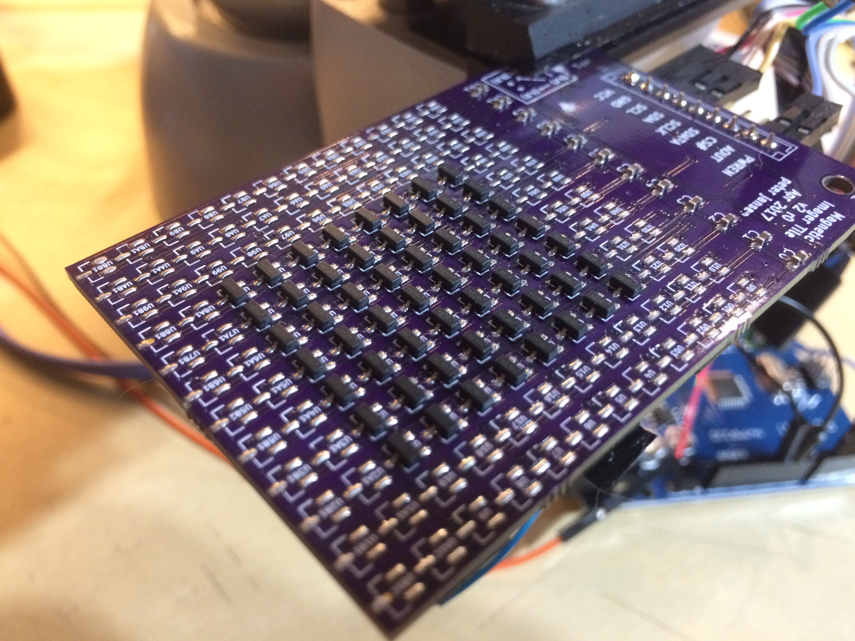
The board itself had very small 6 mil traces, which lead to some manufacturing issues. I was able to cut around the bridged traces and wire-wrap fixes, and populated about half the array for testing:
The bottom of the array, with the analog multiplexers:
Frame Rate
I ideally would like an imager with a high (~1000fps) framerate, to be able to visualize interesting high-speed fields, like the fields oscillating in a transformer. While the 14-bit SPI ADC on this board can achieve about 100KSps (or about 700fps maximum), the I2C multiplexer is much slower, and would likely need to be replaced to achieve high framerates. With the Arduino Uno sample code streaming to the Processing visualization (in the youtube video), it's able to sustain about 10fps, and the Raspberry Pi python example achieves about 30fps after increasing the I2C bus from 400KHz to 800KHz. This could likely be increased a bit with some streamlining of the code.
In terms of slow/static fields, it seems pretty easy to find the speakers/vibration motors in cell phones with the current iteration. The neatest picture that it's rendered so far is of someone's open air pod charger -- lots of magnetic fields of different directions to hold in the ear bud headphones while they're charging, I suspect!
Schematics, Design files, Example Code
Available on Github: https://github.com/opensensinglab/magneticimager
Bill of Materials, Approximate Cost
- After looking through the datasheets for nearly every inexpensive hall effect sensor I could find, I settled on the DRV5053VA, which seems to be a good balance of sensitivity and cost. It's range is only +/-9 milliTesla (on the order of about fridge magnet strength), where are most other sensors are +/-100mT, which means they would be much less sensitive to the smaller everyday fields that are more interesting. For larger fields (like those serious neodymium magnets in the video) you can always hold them further from the imager, but if the sensor isn't sensitive enough in the first place, there's no easy way to detect the smaller fields. The DRV5053VA only outputs from 0-2V (1V center = 0mT), but it has a wide input voltage range, and seems very tolerant to mishandling (it's made for automotive applications). Octopart shows that the DRV5053VA tends to get to about ~0.34 in QTY>1000, or about $49 just in hall sensors.
- Analog MUX ( CD74HC4067M ) is $0.60 in QTY100, so about $6 per board.
- I2C I/O Expander ( MCP23017T-E/SO ) is about $1 in any quantity (but, replace this for faster operation)
- The onboard 14-bit 100KSPS ADC (AD7940BRJZ) is expensive, at about $10 in QTY100.
This puts the BOM at around $70 for the 12x12 imager in modest quantities. Making a single board costs about $200.
Thanks for reading -- and apologies to be slow on updates, Iteration 8 is going much less quickly than I expected. This is my first year as a tenure-track professor, and it's largely an all-day every-day job (which I do gladly, it's very rewarding -- it just means there's less time for other projects, which move a little slower than I'd like).
Discussions
Become a Hackaday.io Member
Create an account to leave a comment. Already have an account? Log In.
Amazing project! I loved your demo at Penguicon earlier this year. In regards to 6 mil traces, that is within our 6 mil trace / 6 mil space spec for 2 layer, so it does appear this is our fault. Please email support@oshpark.com if you ever have an issue. We intend for our customers to get perfect PCBs and will re-make when issues like this. Thanks, Drew Fustini <drew@oshpark.com>
Are you sure? yes | no
Hey Drew! No worries at all, I had already e-mailed support shortly after, and it was all sorted out. The OSHPark boards are wonderful, fantastic quality, and I've used you guys for dozens of boards. No board house can be perfect, so one bad board over five years isn't bad at all. :)
Are you sure? yes | no
Out of curiosity, why not use a 3 axis magnetometer for each pixel. You could use color to represent the vector.
Are you sure? yes | no
I built one out of an array of 3 axis magnetometers a few years ago ( https://hackaday.io/project/5030-low-field-mri/log/15914-concept ), but it's very hard to get as high a pixel density, and also very hard to manufacture something with such tight tolerances over such a large scale without a proper pick and place/solder printer. The 4x4 one was small enough for me to build successfully, but the 8x8 ended up a very expensive coaster. I stlil think it'd be neat to do this with an array of 10x10 or 16x16 MLX90393s, if I could figure out a way to get the density up and inexpensively manufacture it. At 16x16 with magnetometers it'd be about $1000 per board, successful reflow or not... :)
Are you sure? yes | no
the same thing but using array of TLV493D with 5mm pitch:
http://www.desy.de/~vagin/immw20/MagnetSorting.pdf
There was no need for high FPS, therefore all the sensors share the same i2c bus with single address and addressing done by SN74LVC1G08 under each sensor that just activates power when row/column selected. 32 row/col lines are made by TCA9555 sharing the same i2c bus.
Are you sure? yes | no
Neat! That's a really good density, too! I also tried the I2C path ( https://hackaday.io/project/5030-low-field-mri/log/15914-concept ), but had an array of I2C multiplexers to go with the array of magnetometers so that one could do fast/simultaneous measurement.
Are you sure? yes | no
TLV493 is cheaper than MLX90393 and could measure higher fields. however MLX90393 has better resolution.
for the multiplexing additional few cents per logic gate that powers individual sensor does not really affects costs.
but for the readout speed i guess better option would be just to connect I2C SCLK parallel in columns, and SDA parallel in rows.
multiplexing 16 sensors still should be enoungh to have a kHz readout.
and 16 sowtware i2c almost any mcu could handle.
>very hard to manufacture something with such tight tolerances over such a large scale
Also I just soldered them manually, and positioning inacurracy was calibrated out by placing the array into the uniform field and calculating calibration 3x3 matrix for each sensor that corrects for the gain error and also crosstalk from angluar mispositioning of individual sensors
Are you sure? yes | no
Hi, cool project :)
I've been working with Hall effect sensors recently, and was pretty disappointed by the (very) noisy output of the DRV5053 sensors. Maybe it was my setup (a 8 sensors line "array" connected to a PCB with very thin enamel wire, probably a good antenna), but I then bought AH49 (manufactured by Diodes). The quiescent output is 2.5V and go +/- 1 V when exposed to magnetic field, which makes them way less sensitive to noise. And the noise indeed almost disappeared (from https://ibb.co/jA4VxF to https://ibb.co/cT9kWa).
They are indeed less rugged than the DRV5053 but did the job wonderfully.
Also, if you wanted to bring a new dimension to the project, you could use 3D Hall effect sensors (such as Infineon TLV493D).
The configuration of so many sensors would be a pain in the butt and would require more components (I2C MUX or other), since you can only configure 8 I2C addresses.
Good luck with the following of your project!
Are you sure? yes | no
Hmm, that's interesting, I haven't noticed much noise with these DRV5053s. My primary reason for choosing them is that they were the most sensitive, and also low enough cost in volume that it makes constructing large arrays possible. There aren't any units on those scope traces, but the first one looks like very periodic sinusoidal noise, so I'm guessing your guess about the enamel wire antennas is probably correct, and that you may be picking up the 50/60Hz noise from the power lines.
I agree, it'd definitely be wonderful to figure out an easy way to address a large array. The speed of I2C makes it fine for a few sensors, but if one had 256 3-axis sensors on a single bus, it unfortunately likely wouldn't be possible to get very fast framerates. For that, either SPI, or analog sensors (with a fast ADC) would likely be the way to go. This design here is close -- I think if the I2C multiplexer was replaced with something like a regular old shift register (assuming the sensors have protection diodes on their outputs), then one would likely only be limited by the speed of the sensors and ADC.
Are you sure? yes | no
Oh my bad, I should have specified the setup a bit more. The Y-axis is the output voltage and the X-axis is the number of samples ( I used a serial plotter software [Thanks https://hackaday.io/project/5334-serialplot-realtime-plotting-software]). In my setup, I have a cart moving in a translation. On the cart are two magnets, side by side, with opposed polarities (one with N facing the sensor, one with S facing the sensor, shown here https://ibb.co/gxBVGa). Each magnet creates a half sine wave, and by placing them side by side with just the right distance, you get a full sine wave that you can then inverse with asin and obtain the translation position (https://ibb.co/j5gVGa). (tl;dr: The sine wave is intentional, it's not noise).
What's weird is that the AH49, with exactly the same setup, didn't have that background noise.
About the speed, using I2C with a lot of sensors would be much slower, but, if I may ask, why do you want to reach 1000fps (specially if you simply display it and are not humanly able to see at that frame rate)?.
The only point (IMHO) in such a high frame rate would be visualizing a moving field, such as in a motor.
Are you sure? yes | no