 Caleb W.
Project Goals
As a amateur mineral collector, I was recently in the market for a portable geiger counter to identify radioactive minerals. There are dozens of off the shelf geiger counters and kits that would work just fine, but they either seemed too expensive or less-than-eyecatching. Of course, this is the perfect reason to throw practicality out the window and make one from scratch. Before getting into the design, I made a list of boxes this geiger counter had to check.
- Portable, ideally pocket sized
- Low power operation from commonly available batteries
- Reasonably sensitive for detecting weak radioactivity
- Discrete component design for nostalgia's sake and a bit of a challenge
Ideally, I would have used all BJTs for ruggedness and resistance to EMP, but I couldn't get the efficiency of the circuit where I wanted it without using a few MOSFETs.
Schematic Overview and Theory of Operation
Starting on the left side of the schematic, Q7 and Q9 form a classic bistable multivibrator which oscillates at roughly 22kHz. This keeps audible noise to a minimum while prioritizing electrical efficiency. The benefit to this type of oscillator is the relatively fast turn off time of the transistors. I found a good balance of resistor and capacitor combinations that have a fall time under 75nsec, which will maximize the amount of energy extracted from the inductor every cycle. These pulses are fed into Q2 via a high pass filter which limits the current pulses through the inductor to 3uS. This is important to keep the main inductor out of saturation, which will waste energy. Also, if the oscillator gets stuck 'ON' for some reason, there is no risk of dumping current through the main inductor. When Q2 is pulled low, Vbe of Q5 drops below 0.6V, and charge from the main MOSFET gate gets pulled to ground via D3. As soon as Q2 turns off, R9 and Q5 form a voltage follower which turns the MOSFET ON. R6 prevents unwanted oscillations in the gate voltage.
When the current is cut off from L1, the inductive EMF kickback is fed through the secondary side which adds the two voltages together. This high voltage spike goes through D1 and begins to charge the main high voltage capacitor. R5 and C5 form a snubber network that technically isn't needed, but without it, there is a lot of ringing on the FET drain which will cause a lot of unnecessary RF noise. The efficiency hit is pretty minimal, and it's the 'right' thing to do. The voltage across C1 is sensed via a resistor divider network consisting of R2, R3, R4, and R7. 100Meg resistors are needed here so the leakage is minimal. At 400V, even a 10Meg divider will be the main loss of power in this circuit. 100Meg resistors are a decent balance between leakage current and cost.
When the voltage at the base of Q3 reaches the setpoint of 0.7 volts, it begins to conduct. The setpoint voltage can be adjusted via VR1. This lets you use a 100k adjustment pot, which is easier than trying to find a 10Meg pot. A crude voltage regulator consisting of R19, D6, and C12 provides a relatively stable 3.6V for a consistent output voltage across the entire battery discharge range. The collector current in Q3 is amplified by Q4, and inverted by feeding the collector current from Q4 into Q8 and Q10. Even the tiniest base current into Q8 pulls the gate of Q6 low, cutting power to the oscillator circuit. This lets the high voltage capacitor slowly discharge through the resistor divider. As soon as the high voltage line drops slightly, Q6 will turn the oscillator back on, forming a negative feedback loop. Very high loop gain is preferable, as it improves load regulation and response to transient current draw from the geiger tube. R17 and C7 form delay circuit which forces the whole circuit to squegg. While this does cause some ripple on the output, overall efficiency is much better. Q10 conducts when the regulation loop is active, so D2 will light when the output is in regulation....
Read more »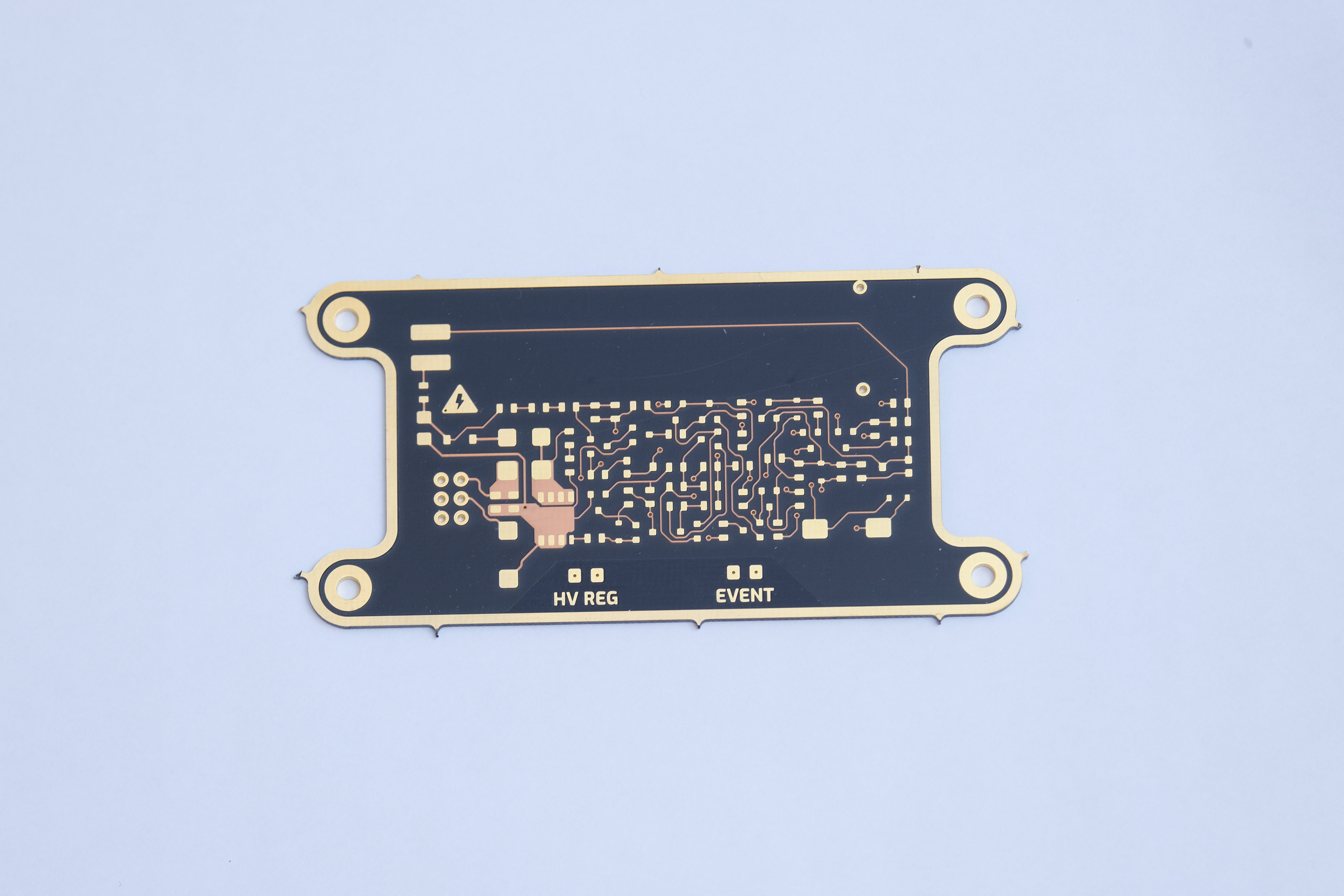


 James Wilson
 Kuba Sunderland-Ober
http://forum.rhbz.org/topic.php?forum=2&topic=87
Simple one. Works fine