 Reed Foster
One advantage of a-IGZO transistors is the simplicity of fabrication: for the top-gate, top-contact devices used in this project, only 3 photolithography steps were needed (4 steps can be used to make a bottom+top-gate 4-terminal transistor process with the extra benefit of 2 metal layers), and the biggest advantage: low temperature processing (highest temperature step is a <400C rapid thermal anneal). However, the main disadvantage of amorphous thin film transistors in general is their relatively poor mobility (1-50 cm^2/V/s vs. 1400 cm^2/V/s for Si or >10000 cm^2/V/s for graphene films). Furthermore, for IGZO specifically, the inability to construct strongly p-type material precludes the creation of complementary logic.
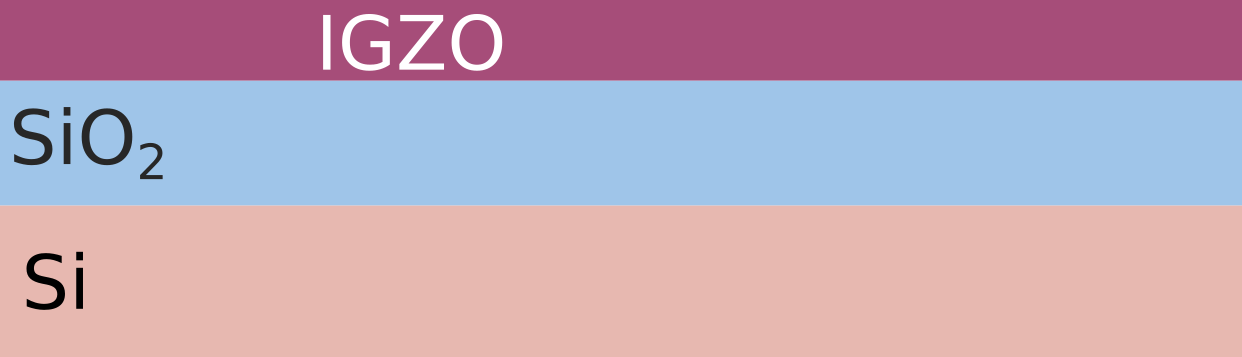
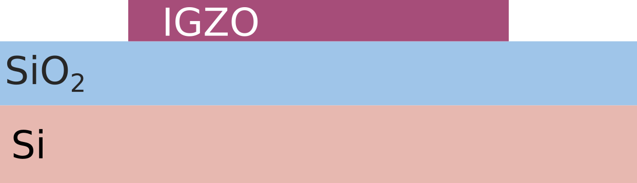
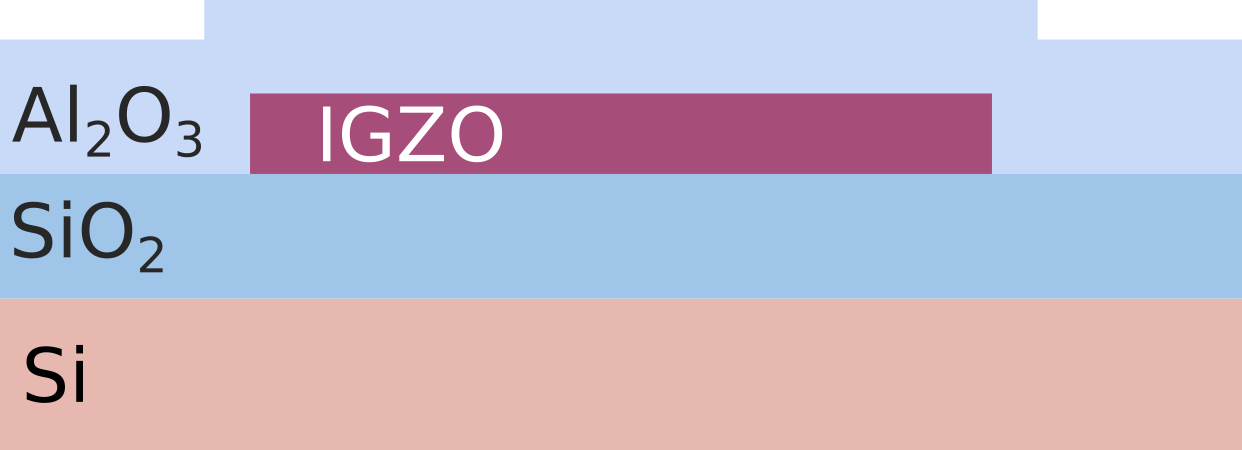
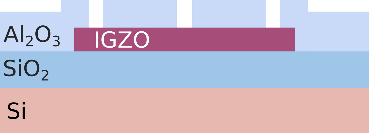
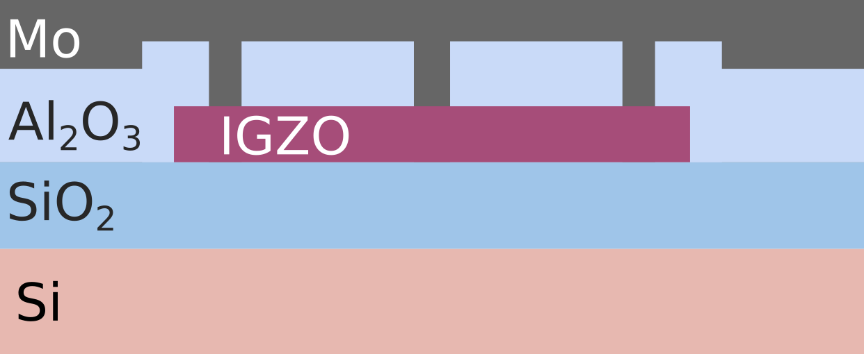
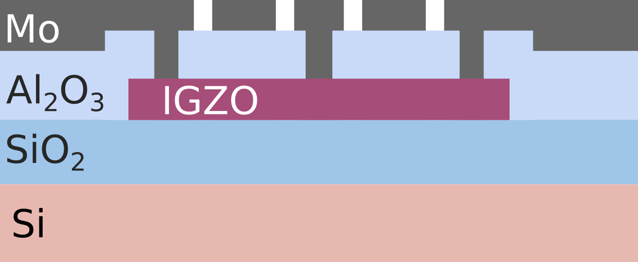
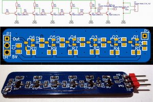
Fabrication of a transistor pair
 |  |
 |  |
 |  |
 |  |
Preliminary Testing
In order to verify that the fabrication went smoothly, I fist measured the current-voltage (IV) characteristics of a single transistor. First, I verified that the contact between the molybdenum and the channel was intact by measuring the IV characteristics of the device when ungated. Then, I verified the presence of a field effect by setting the drain source voltage constant and sweeping the gate voltage until an exponential decrease in current was observed (due to the materials used and the composition of the IGZO target used for sputtering, this device was depletion-mode, meaning that it's normally on when no gate-source voltage is applied, and a negative gate-source voltage is required to turn the device off). Below is an example transfer characteristic (current density vs. gate-source voltage), plotted on both a log and linear scale.

Small Signal Modeling
In order to accurately model the behavior of the amplifier for small signals, I constructed a small signal model (a linearization of the transfer/output current-voltage characteristics of the transistor about some operating point). The small signal model for TFTs is a bit different from that of conventional MOSFETs because the dominant parasitics are different. In a conventional MOSFET, the device generally has large overlap capacitance and small contact resistance, while in a TFT, the contact resistance often dominates the performance and the overlap capacitance is small. Below is a sketch of all of the parasitics present in the IGZO TFT:
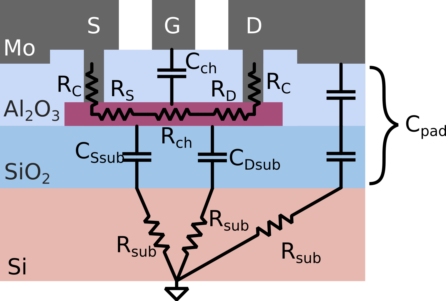
In reality, the effect of the capacitance of the IGZO channel to the substrate is pretty negligible, since most of the charge flows near the top of the IGZO film and the material is highly resistive. For the device I fabricated and measurement setup I used, the dominant capacitance was unfortunately the capacitance of the cable connecting the probe station to the oscilloscope (this happened because I didn't think to insert a large resistor in series with the measurement apparatus and the amplifier output --- this is why using probe tips with your oscilloscope is very important!).

 Ben Holmes
 engineerkid1
 Tim
Tim
Cool project. I hope to see more of such transistors embedded in everyday artefacts.