 Ricardo Tonet
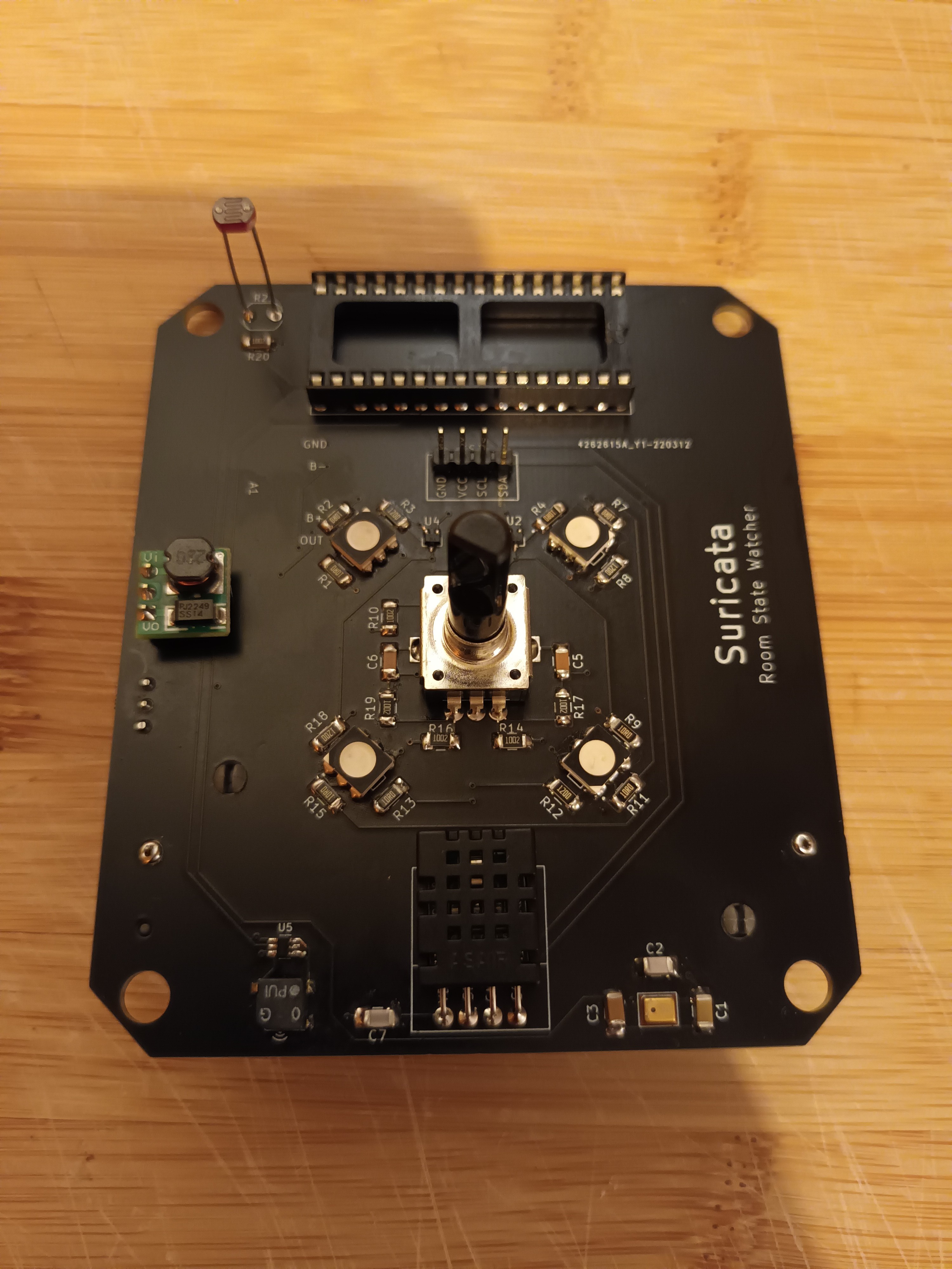
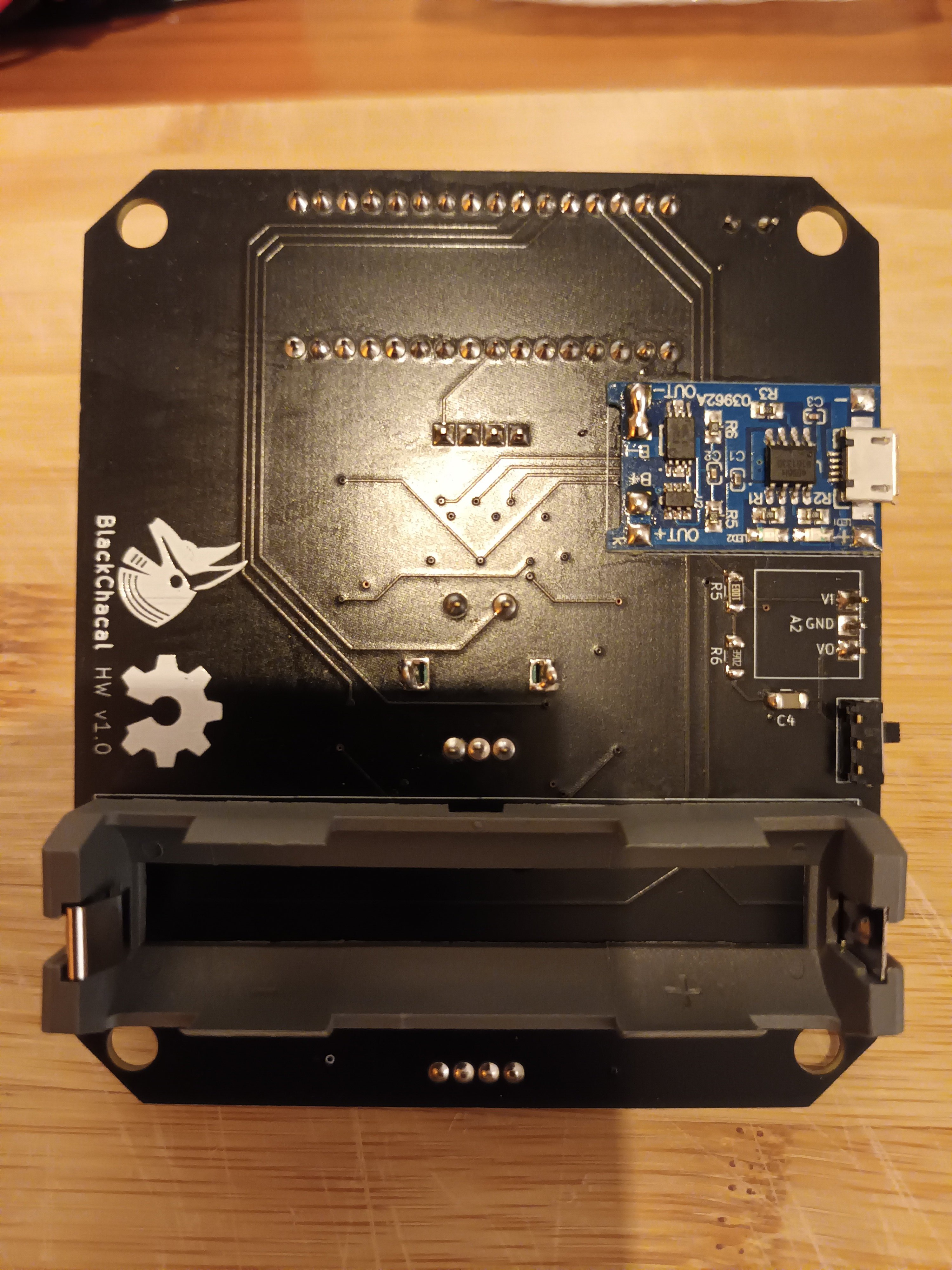
Finally I have my PCB assembled. I took me a while because I was assembling 5 PCBs at the same time, although, only one is complete. I did not buy all the components for the five of them. I will later on.
During assembly I also noticed a few mistakes on the PCB. The component A2 is a boost step up breakout board to 5V. I switched the Vin and Vout pins on the back footprint, so I had to solder the component in the front.
The component A1 is a LiOn battery charger breakout board. I forgot to connect the GND to the battery (-) connector on the schematic and PCB. I ended up making a solder bridge between the two pads directly on the breakout board. I tested the Power supply and it seems fine. This component also has the pad description footprint showing on the front instead of the back.
I already started the final fw with arduino on the breadboard. After fully testing the board I will start to develop directly on the PCB.
Here are the assembled PCB pictures:
Discussions
Become a Hackaday.io Member
Create an account to leave a comment. Already have an account? Log In.