0%
0%
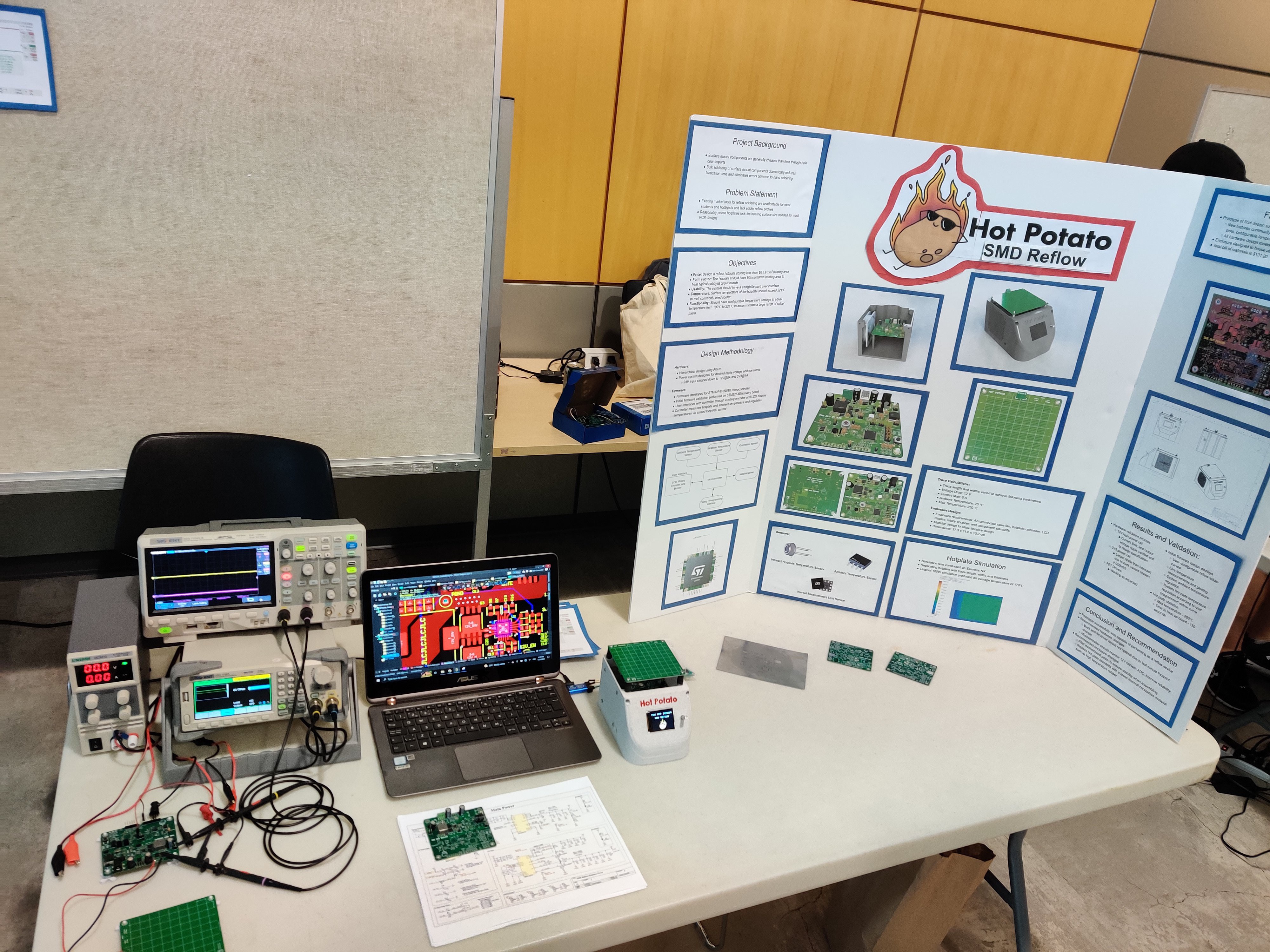
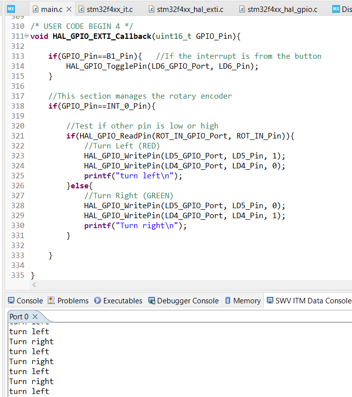
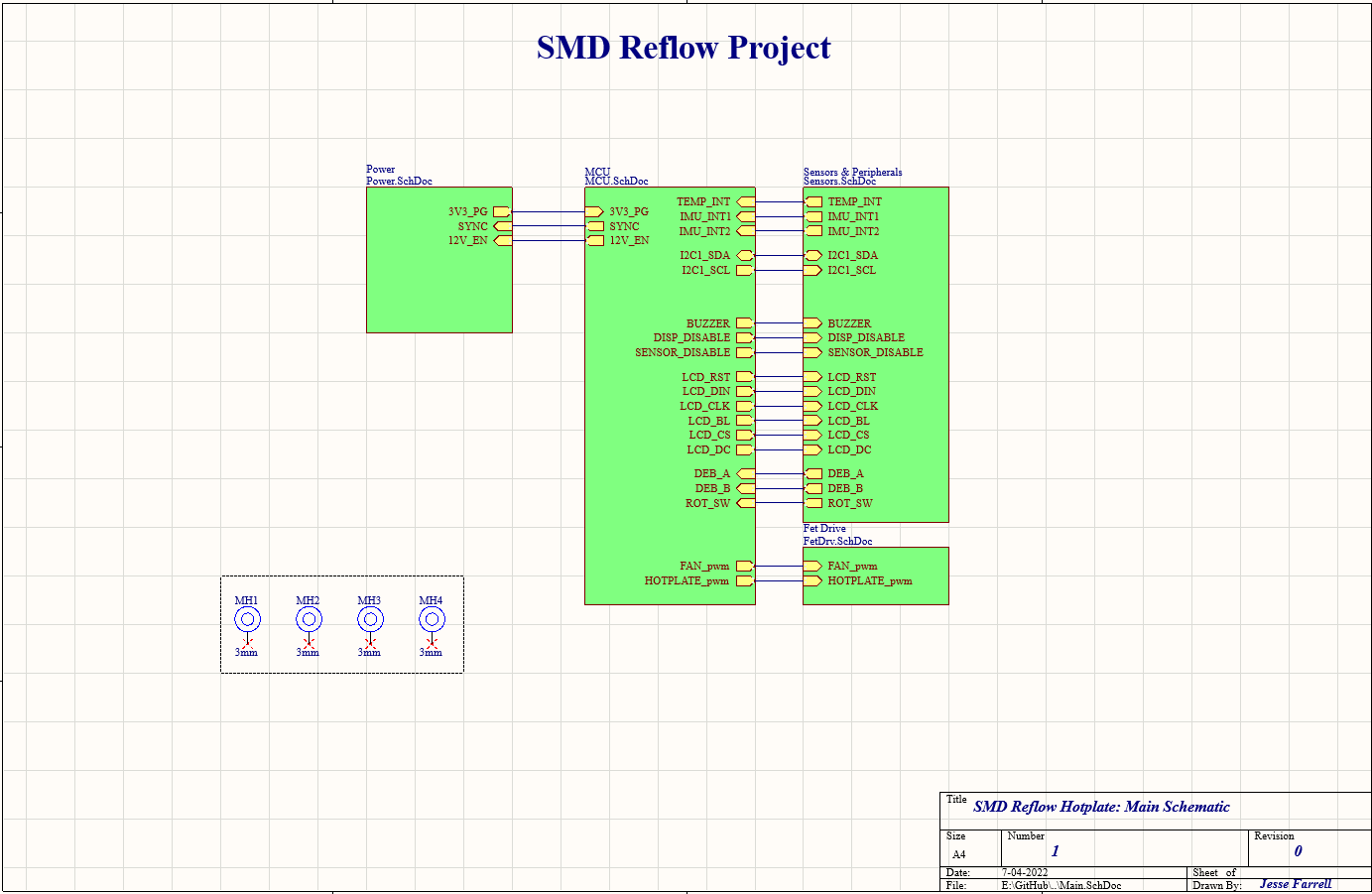
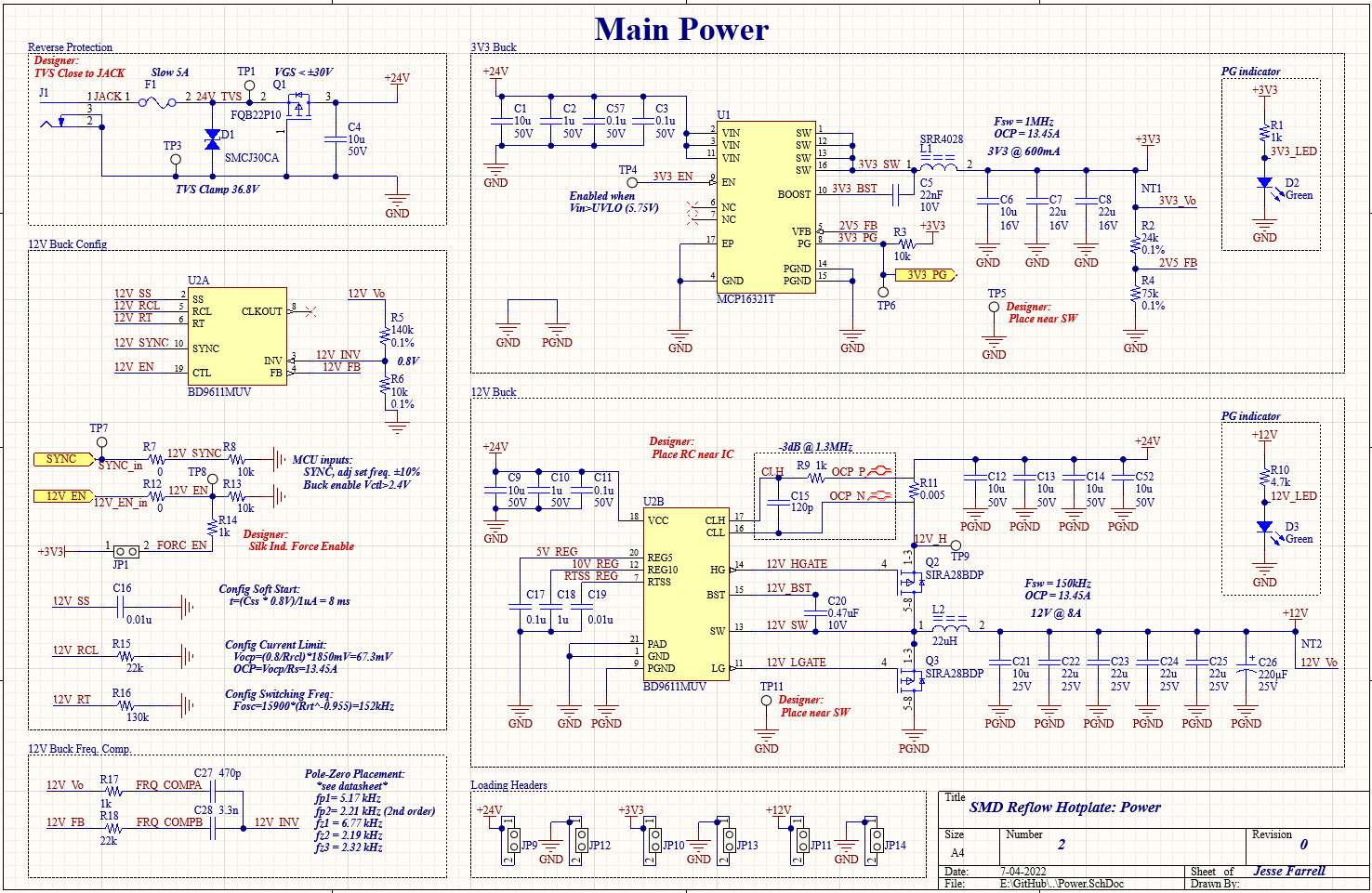
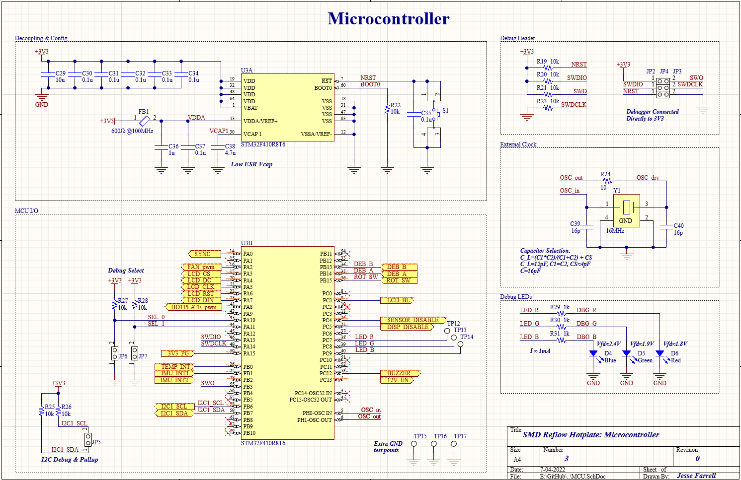
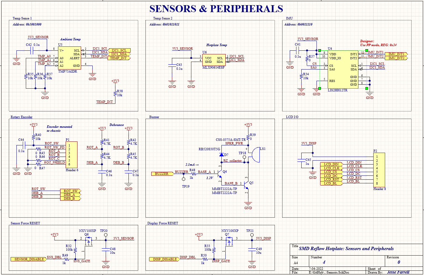
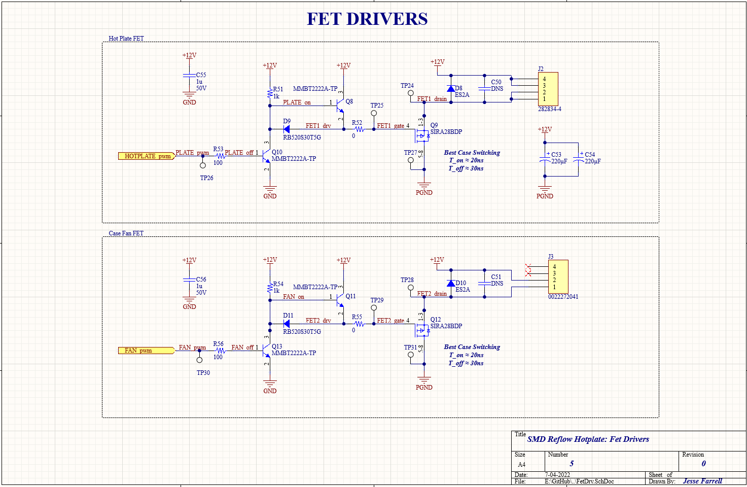
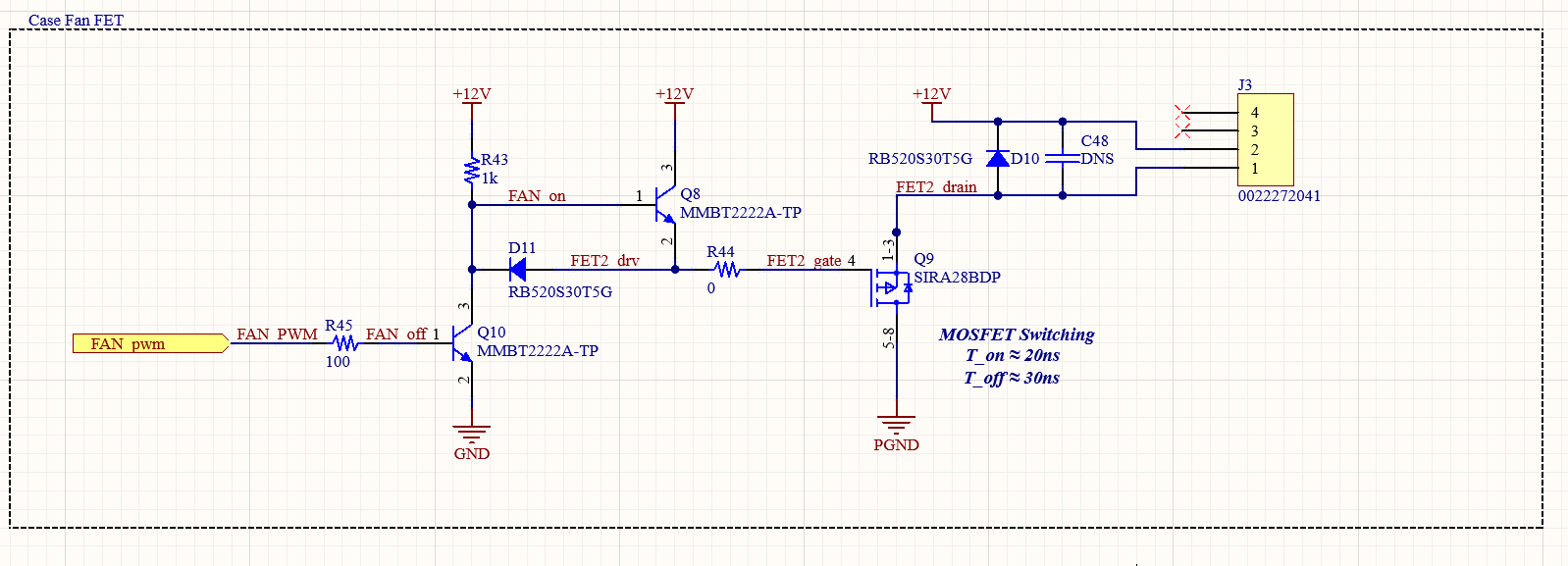
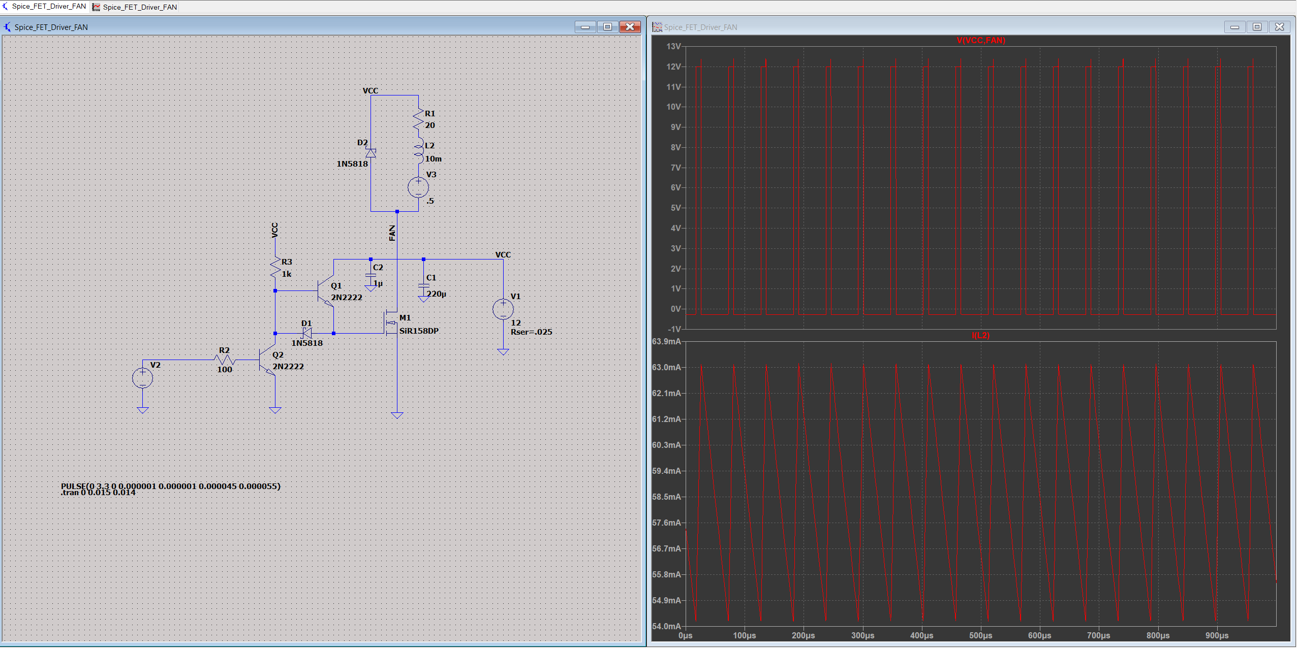
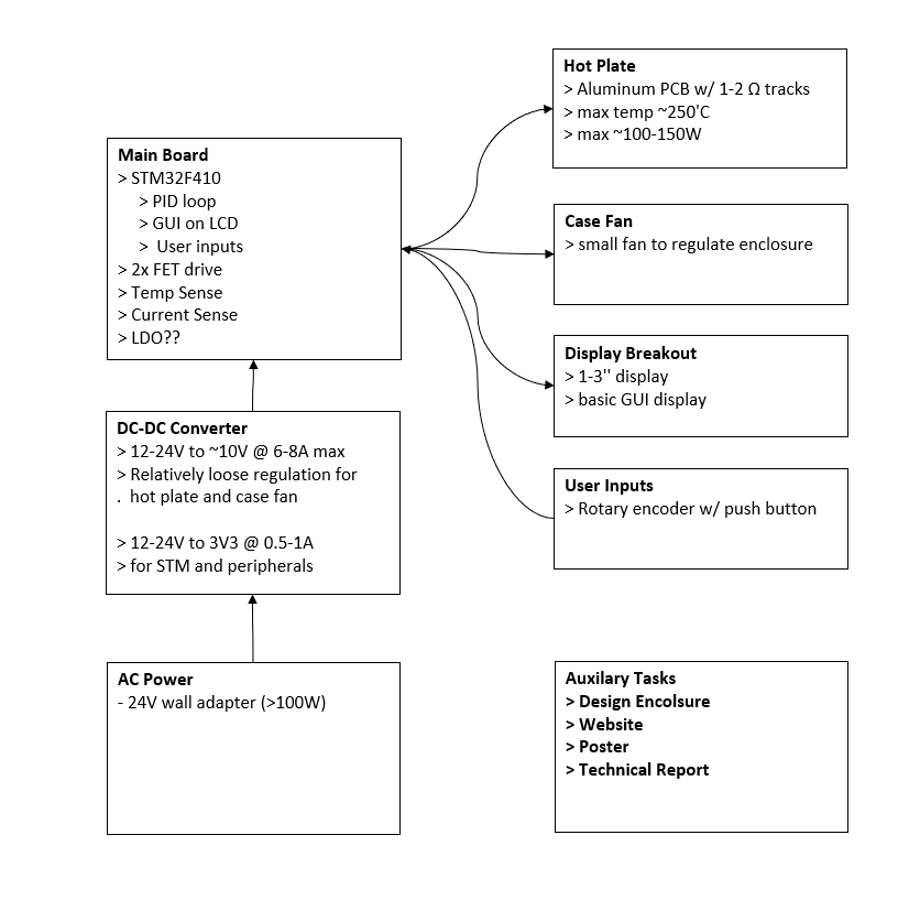
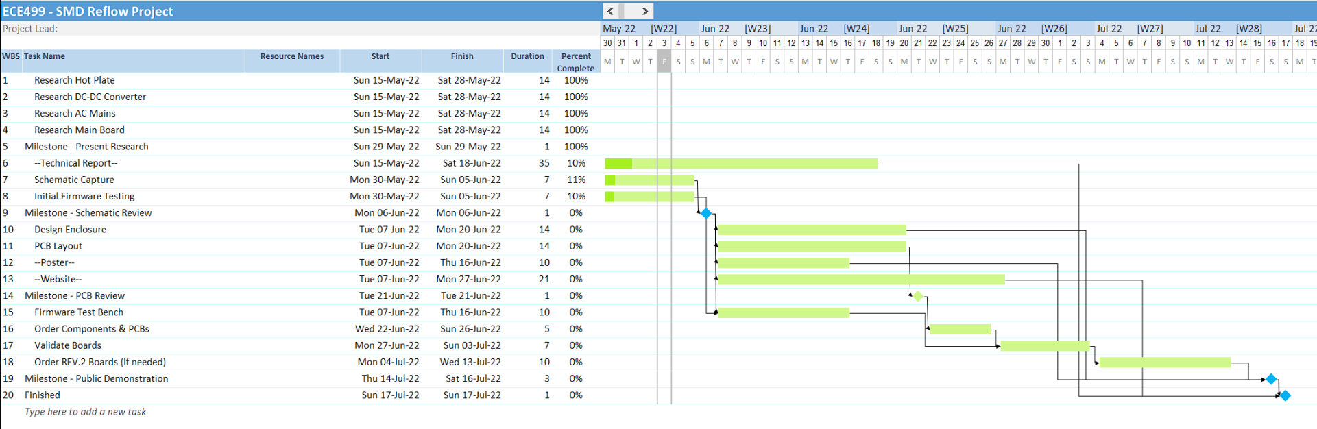
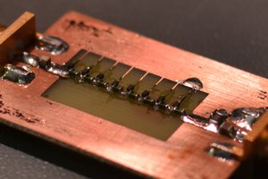
SMD Reflow Hotplate
Open Source SMD Reflow Hotplate for small PCBA
Become a Hackaday.io member
Already have an account? Log in.
Just one more thing
To make the experience fit your profile, pick a username and tell us what interests you.
Pick an awesome username
hackaday.io/
Your profile's URL: hackaday.io/username. Max 25 alphanumeric characters.
Pick a few interests
Projects that share your interests
People that share your interests
 Logan Cummings
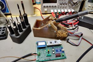
 Tyler Ward (Scorpia)