The widget needs two identical FET driver circuits to help switch regulate the current through (a) the case fan, and (b) the Hot plate itself. The drivers will be controlled by a logic level signal. If we try to control the FET without the driver circuit, the FET would be switched inefficiently if at all (slow switching leading to switching losses, and insufficient drive leading to higher Rds_on). For BOM consolidation the two FET’s will be identical (This leads to a very overkill FET for the fan). The schematic for this circuit is shown below. Since the FET will be driving an inductive load a flyback diode was added across the power terminals to avoid.
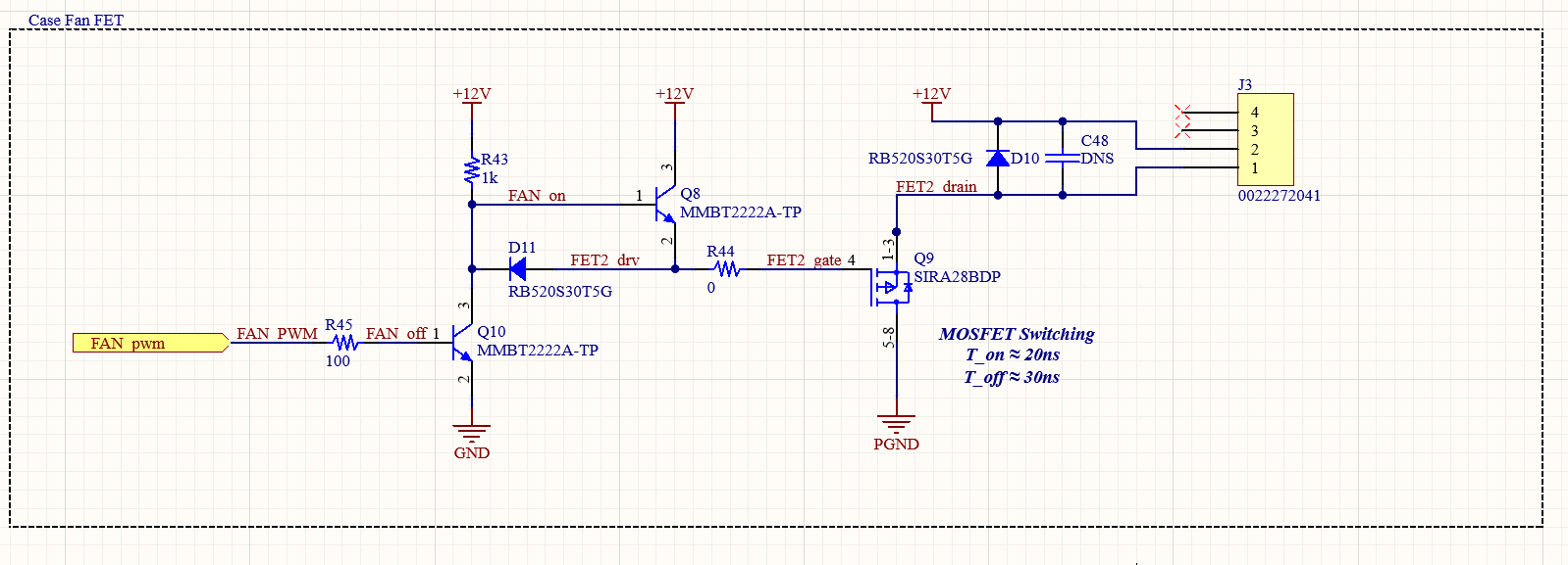
This circuit works as explained below. When the input signal (FAN_pwm) is high the lower BJT is on (Q10). As a result, the base of the upper BJT is pulled to ~GND, and the gate of the FET is drained. When the input signal is low the lower BJT is turned off, allowing the upper BJT to turn on and charge the gate of the FET.
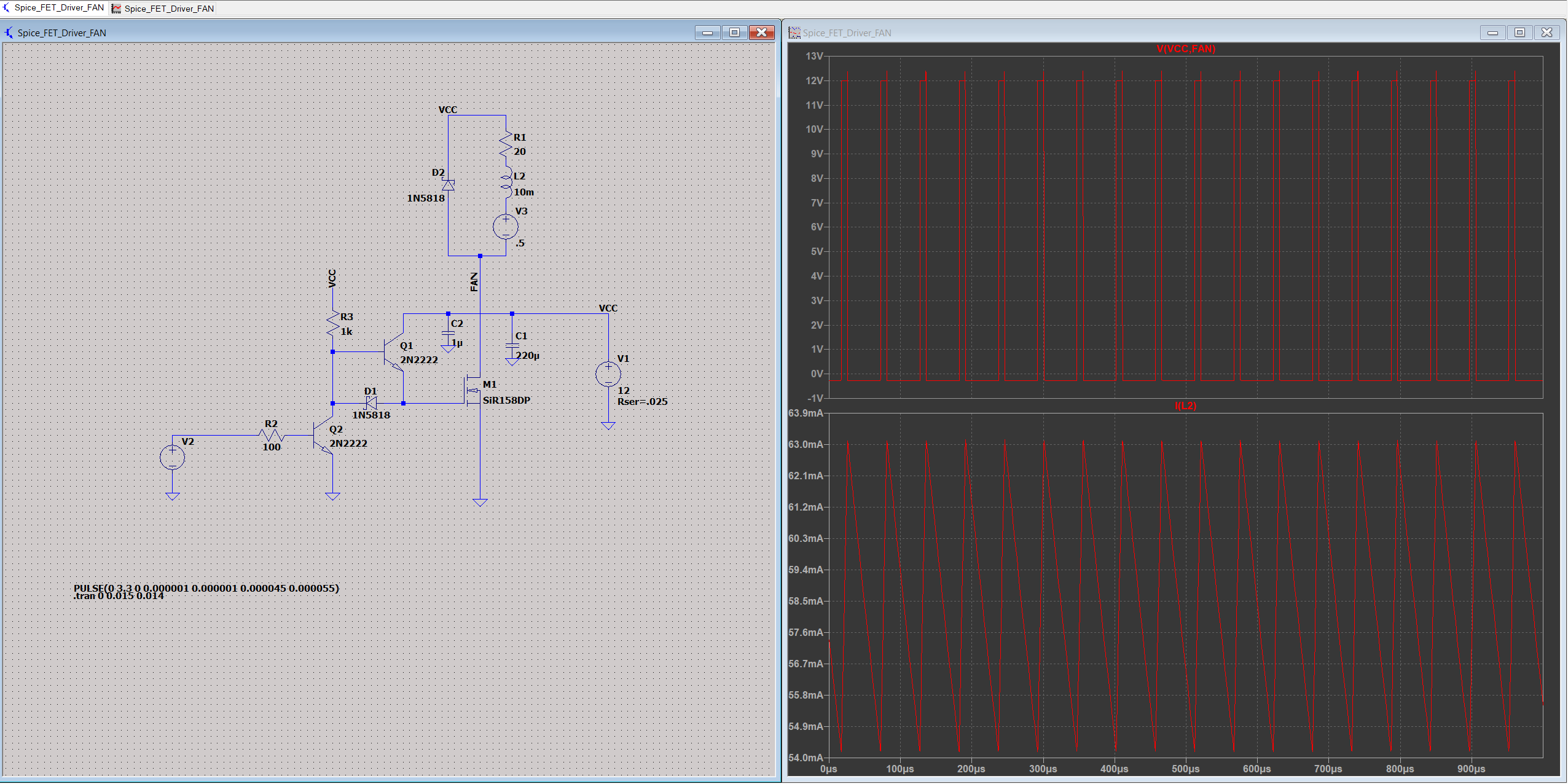
Here is a basic simulation of the circuit using some generic components. I used this to help confirm my understanding of the circuit, as explained above.
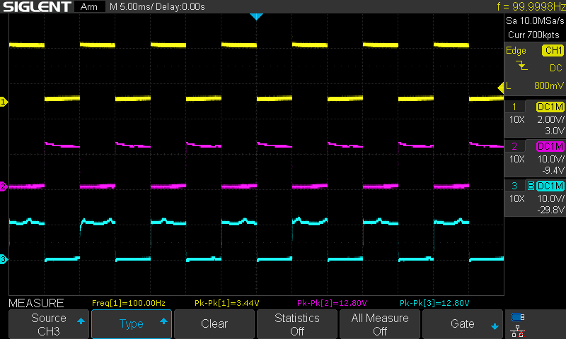
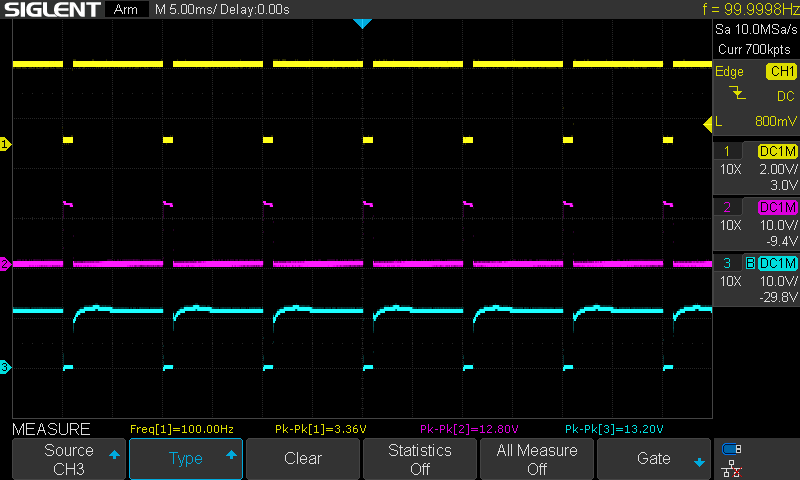
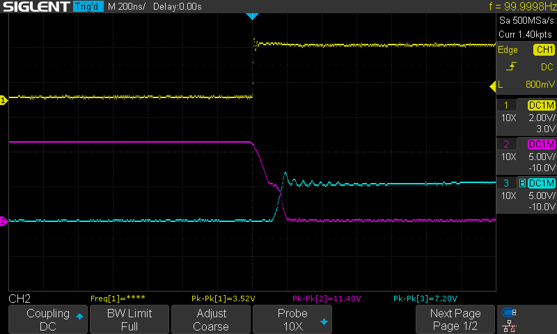
The circuit was also configured on a breadboard. I was curious if there would be any “coil whine” from the FAN (I’ve had issues with this in the past), and at what frequency the FAN should be driven. 100Hz seems to work well with this fan. In the screen captures below, CH1 is the input from a function generator, CH2 is the gate drive, and CH3 is Vds.
Here its being driven at 50%.
And here at 90%. The Fan is barely going at 90% duty cycle (note logic is inverted so this is 10% on).
Lastly, the transient. Ideally I’d have a the drain current as a waveform here, but I need to solder up a CSA for high current to make that measurement (and I’m waiting on some SMD potentiometers for that project).
Discussions
Become a Hackaday.io Member
Create an account to leave a comment. Already have an account? Log In.