School’s been fairly busy over the past bit so I haven’t had much of a chance to add any posts here. In this log, I’m going to dump a basic overview for the various sheets of the SMD reflow hotplate project. This board is the controller board, it will connect to a passive hot plate made from an aluminum PCB (testing on that to come).
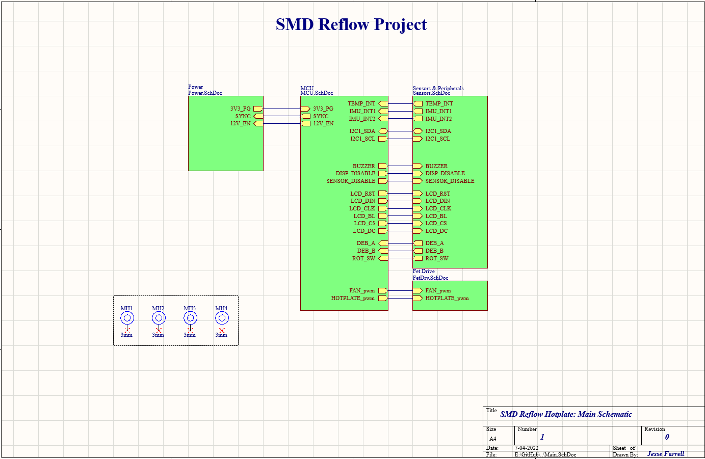
The first sheet contains all the hierarchical blocks. I split the schematic into 4 sections, power, microcontroller, sensors/peripherals, and FET drivers.
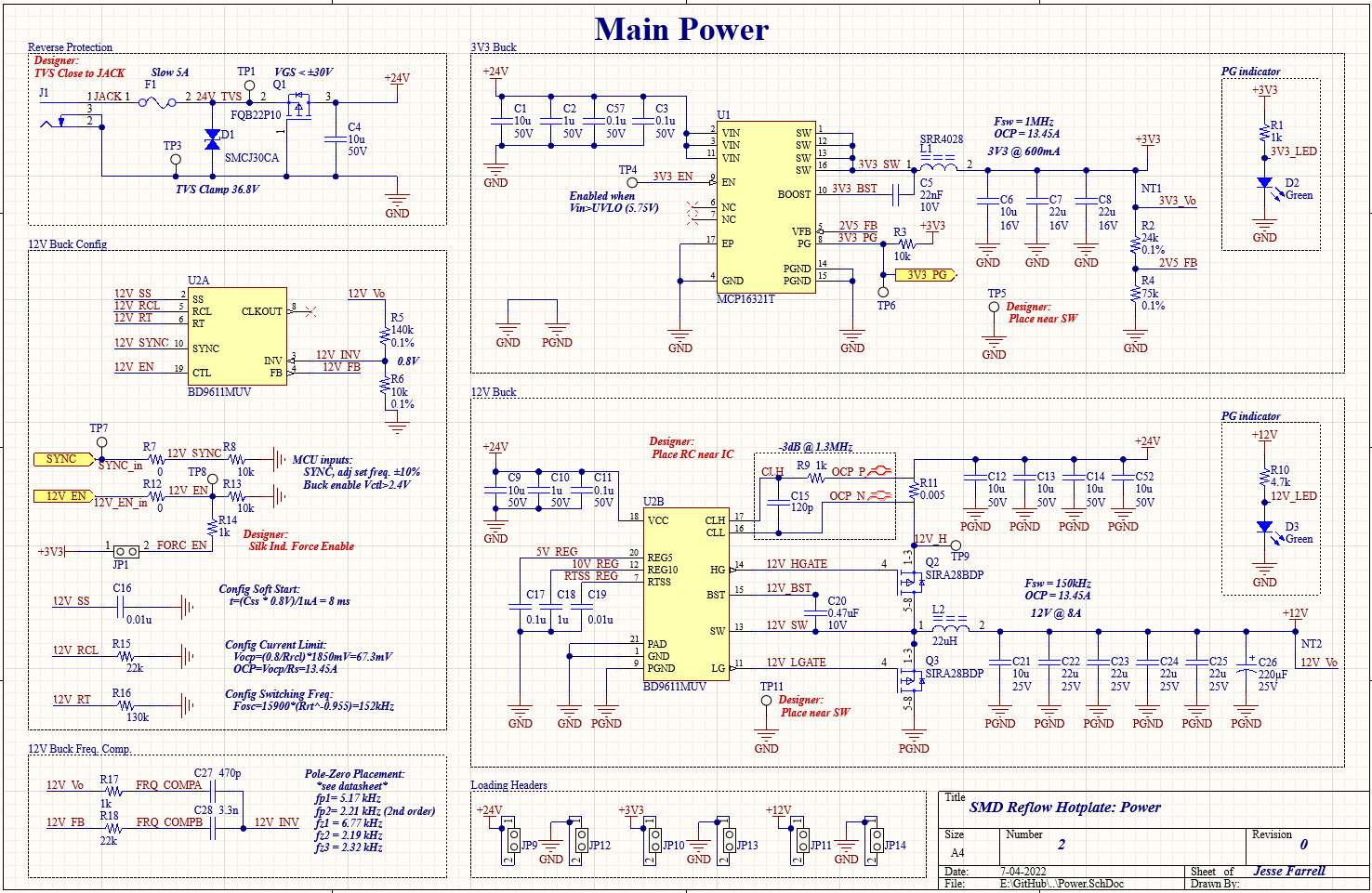
The power block is the largest schematic in the project (I probably should increase the sheet size a bit). It contains a 3V3@600mA and 12V@8A buck. Both these DC-DC converters step down a voltage from an external 24V wall adapter. Originally the hot plate was going to handle AC-DC rectification, but due to the 3-month timeline it wasn’t feasible. I’ve highlighted several sections in the schematic. The reverse protection section provides OCP, OVP, and UVP for the downstream components. It uses a PMOS transistor for reverse voltage protection and a TVS diode for ESD protection. On the topic of ESD, I’m not sure if the FET would survive even with the TVS diode (max Vgs 30V), ideally the PMOS would have a maximum Vgs above the clamping threshold of the TVS diode… but the component shortage won this round. Lastly, yes I’ve shorted GND with PGND without a net tie… I’m planning on tying these nets together with via’s and I couldn’t find a nice way of doing this in Altium. Note, the SIRA28 FET has since been tweaked for a higher power variant.
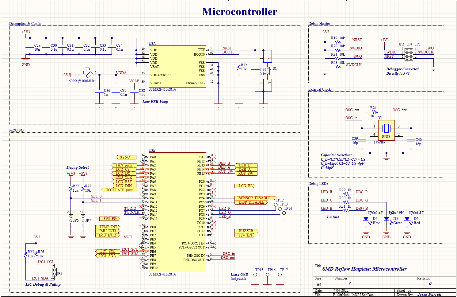
The microcontroller schematic is fairly self-explanatory. We are using an STM32F4 which will drive various pwm signals, run a PID controller, display a basic GUI, and interface with several I2C devices (I managed to swipe some from Digikey awhile back, otherwise this component is fairly unobtanium). Although I originally thought this MCU was overkill, we ended up using nearly all its I/O and most of its timers. To help with debugging I have 2 configurable inputs SEL_0/SEL_1 and 3 debug LED’s.
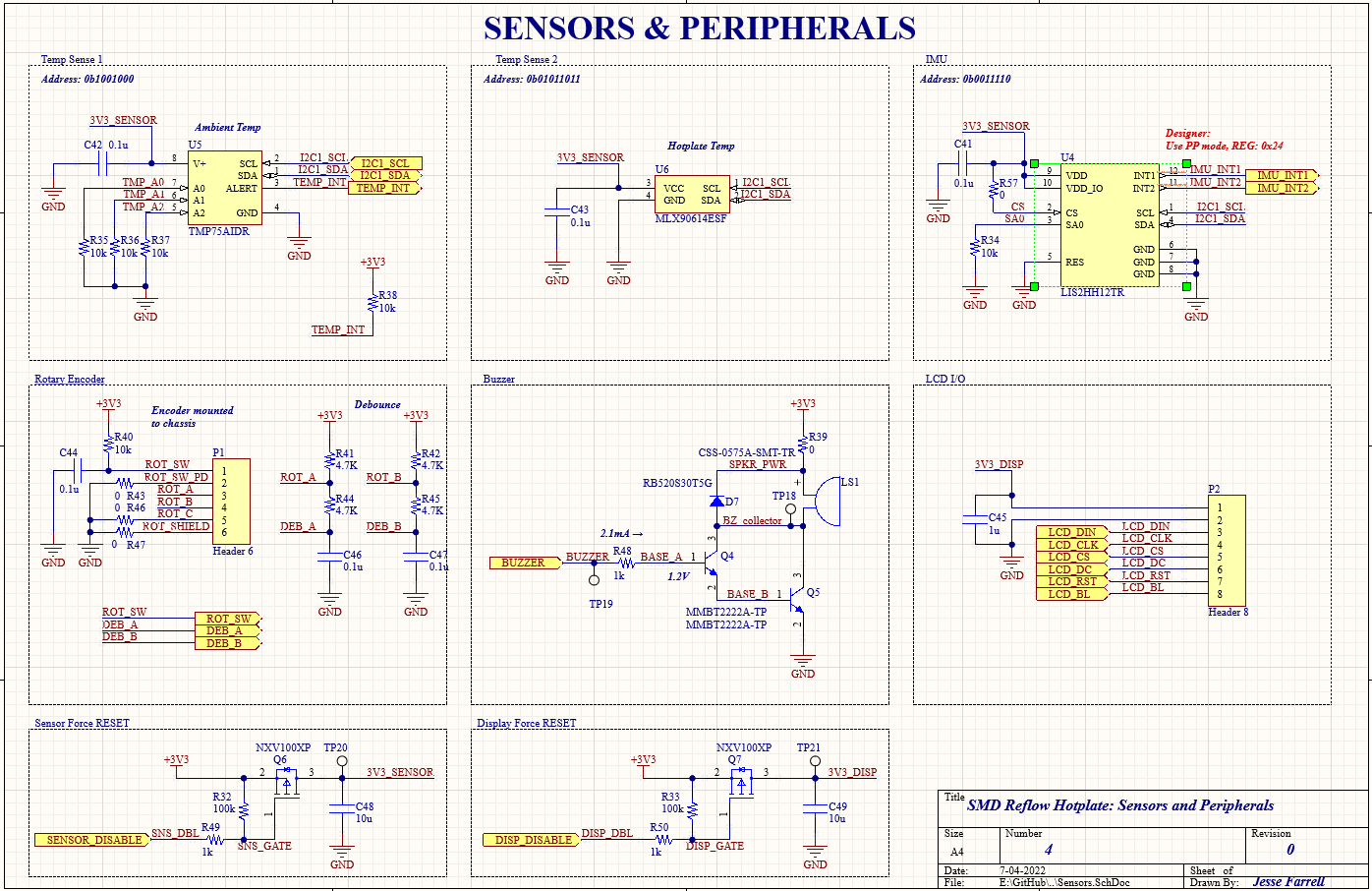
The sensors consist of 2 temperature sensors, one to measure the hot plate via inferred and one for ambient case temperature, and 1 inertial measurement unit (IMU). The IMU was added as an afterthought, I have a couple LIS2HH12TR’s in my parts drawer and I thought it could add some interesting safety features/functionality. These 3 peripherals can be hard reset via a PMOS switch. There is also a rotary encoder, a buzzer, and the LCD I/O. Note that both the rotary encoder, and LCD will be mounted to the case so I’ve just used basic 2.54mm pitch headers. Like the sensors, the display can also be completely disabled. This was included to allow the system to enter a deep-sleep state where all peripherals are switched off.
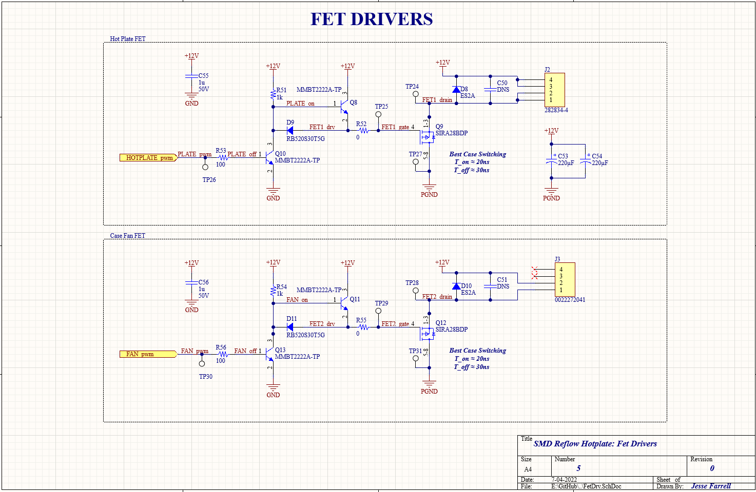
The last schematic is for the FET driver circuits. The FET drivers control DC-DC choppers that will drive a FAN and the main hot plate. Note that these two choppers use the same FET for BOM consolidation. I’ve included several test points so that this circuit can be tested independent of the rest of the system. Note, the SIRA28 FET has since been tweaked for a higher power variant.
Discussions
Become a Hackaday.io Member
Create an account to leave a comment. Already have an account? Log In.