 Emilio P.G. Ficara
Emillotron - part 1
The title is a mix (a crasis) between Emilio (my name) and Mellotron. The Mellotron was used in the 1960s, in the time of the Beatles. In those years, long before “digital music”, someone invented a mechanical system that made a magnetic tape slide in front of a head when a key on the keyboard was pressed, thus reproducing the recorded sound. The device I am about to introduce to you has nothing to do with this… It is always about generating sounds and possibly music, but here we are going to use FM synthesis (this is Frequency Modulation, but it is not a private radio).
Many (MANY) years ago, I started my career as a firmware / software / electronic designer in a company that produced electronic musical instruments (keyboards, organs, etc.) and therefore had the opportunity to get in touch with everything new appeared on the market. When Yamaha came with FM synthesis (theorized by Chowning), suddenly a polyphonic and polytimbral keyboard could be created with a single chip! Of course, there was a lot of study to be made, but I love doing it and so, together with the music consultant, I “hacked” the registers of the chip to get decent and sometimes even indecent sounds, like alien calls!
Well, I found this prototype in my garage, almost empty. It was probably a test board, because there are a couple of flying wires underneath. Being about 40 years ago, I don't remember the details, but in all likelihood I had designed the card with the Rockwell 6502 micro (the legendary one) since at that time I was using an Apple II as a development system.
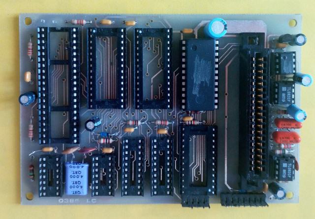
The only integrated chips left on the board are those related to sound generation, therefore the OPL-II chip, the DAC and two opamps with buffer and filter functions. Note that in those days there was no concept of sharing and everything was done not to be copied by the competitors! In fact, as you can see from the image, the names of the ICs are deleted and it is not an effect of the graphics program, but of a small cutter 🙂
Well, the device that I am about to present is part of a larger project which is an "integral relax machine". In short, this machine will be able to generate visual stimuli (strip of colored LEDs), acoustic (this sound generator) and tactile (boxes to be held in hand with motors that generate vibrations).
For the synthesis of FM sounds, I suggest you read an article of mine from a few years ago at this link: http://ficara.altervista.org/?p=1381 . The article had some success, also because I published the source files in C (converted from my originals in assembler) and everything was even mentioned by hackaday which is a beautiful site for innovative ideas and "hacks" of all kinds.
The project presented then was based on a 40 pin Microchip PIC driving a standard PC sound card (ISA bus, now obsolete stuff). In this new version, I decided to simply use a Yamaha OPL-II chip (YM3812) with an Esp8266 based circuit (mini D1 module) and suitable peripherals (I2C + SPI), developing the firmware (with appropriate conversions from the original) on Arduino platform. If only the OPL-IIs (two operators) are used the code is practically identical for both the chips used on the ISA sound cards and the YM3812.
Let's see what it takes to interface to the OPL-II chip. This is the pinout:
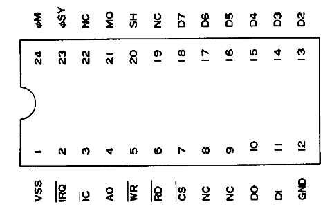
The signals necessary to write the various registers of the chip are: D7..D0 (the data bus); A0 the base address (note: there are many registers, but why is there only one addressing bit? Simple. If A0 = 0 is used, the address of the register to be read or write is sent to D7..D0; if A0 = 1 is used, the previously addressed register is written, so it is a two-step operation). Other control signals are / CS (chip select), / RD (read) and / WR (write). Finally we have / IC which is in effect the reset pin and / IRQ which is the interrupt output signal from the chip, which is not currently used.
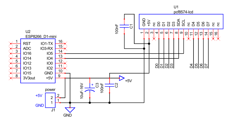
The other pins are for the power supply, for the DAC and for the reference oscillator. How do I connect all these signals to the ESP8266 mini D1 board? Clearly, we need some I / O expansion. I decided to use the I2C interface for the D7..D0 data bus, while the SPI for the various control signals. I have only used material that I had available from previous experiments and so you will see an I2C interface originally created to drive 2 × 16 LCD displays, with slight modifications:
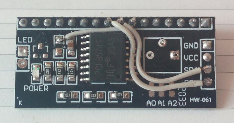
This circuit allows you to control an LCD (character) display via the I2C bus. It uses the LCD controller in 4 bit mode, so with the 8 I/O lines available on the integrated PCF8574T it is able to give all the necessary signals. The changes I made are only used to have all the signals on a single connector, as shown in the diagram below:
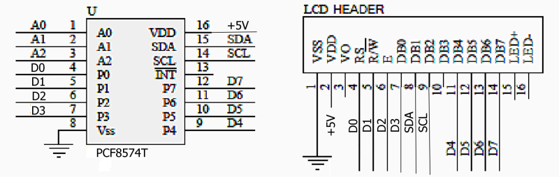
The DB0..DB3 signals of the LCD connector were originally free and are now connected to D3, SDA and SCL instead. The RS, R- / W and E signals were already connected to D0, D1 and D2. The P3 (pin 7 of the integrated) was connected to a resistor based on the transistor that drove the backlight. I removed the unnecessary components and wired up the signals I needed and in this way I now have everything on a single connector. The I/O ports of the PCF8574T are of the “quasi bidirectional” type which means that each line can be used as input or output without having to set a direction register. In practice, to read an input, you must first write a '1' to the output and this activates a sort of “weak pull-up”, which is very different from a push-pull output port. In any case, there is another I/O expansion module via I2C that already has all the pins available on a single connector and if you want you can use that and avoid this modification to the I2C - LCD module. Again, I had this and used it!
In this application I need all 8 bits of the PCF8574 for the D7..D0 data bus and therefore I will have to use a second circuit to expand the I/O and have the necessary lines for the control signals. For now, let's start testing the I2C section. This is the diagram of the connections between the ESP8266 mini D1 module and the (modified) I2c-LCD 8574 module:
Well, now is the time to write the first test program. Here it is:
// Test i2c I/O expander (output mode)

#include <Wire.h>  // this is for PCF8574T
uint8_t wdata; // data write to D7..D0 bus

void setup()
{
  delay(250); // power-on delay
  Wire.begin(4, 5); // begin with PCF8574 (sda, scl)
}

void loop()
{
  Wire.beginTransmission(0x27); // address of PCF8574T
  Wire.write(wdata++); // write to D7..D0 bus then incr. counter
  Wire.endTransmission();
  delay(5); // cycle time
}
The program is really very simple. It writes a byte to the port (i2c expansion) and then increments its value. The result that we will see on pins D0..D7 will be a series of square waves, each with a period double that of the previous pin. Since we used a delay of 5mS, the frequency we will have on pin D0 is about 100Hz (10mS, a change of state every 5mS). Once the source for ESP8266 mini D1 has been compiled and the executable transferred to the module, we will have this result:
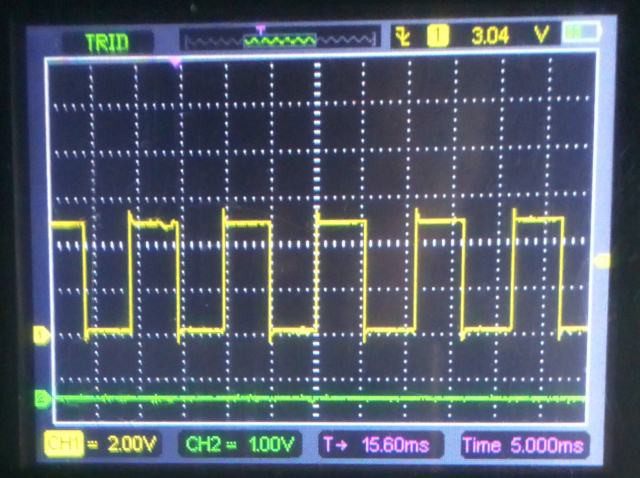
The time of the delay function is not compensated (the duration of the following operations is not taken into account); to get the most precise times it is better to use the millis () function in the loop, but in this case we just need to see if everything works and that's okay. The address of the i2c expansion is fixed at 0x27, which is that of the PCF8574 with pins A0..A2 all at high level (without jumpers).
If we don't have an oscilloscope, we can build this little tool (it will come in handy soon after for testing inputs)
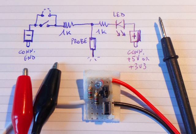
As you can see from the diagram, the LED lights up if we touch a pin at a low level with the lead, as long as the red crocodile is connected to a positive voltage. In this case, since the PCF8574 is powered at 5V, we can connect the red crocodile to this voltage. Since pin D0 switches to 100Hz, if we measure this pin we will see the LED always on (if we are not Vulcanians ...) and therefore it will be better to move at least to pin D2, where we will see a fast, but perfectly distinguishable flashing. The black crocodile will not be connected, or it can be connected to GND, but the jumper must be open, as well as the push button. However, since there is a 1K resistor, there is some protection in case of distractions (I = 5V / 1KOhm), but the led will never be off! Instead, we will have a kind of modulated light,
Now let's move on to testing the input part. Here we have a very small program:
// Test i2c I/O expander (input mode)
#include <Wire.h> // this is for PCF8574T
uint8_t rdata; // data read from D7..D0 bus
uint8_t count; // counter for n prints on the same line
char pbuff[6]; // buffer for formatted serial print
void setup()
{
delay(250); // power-on delay
Wire.begin(4, 5); // begin with PCF8574 (sda, scl)
Serial.begin(38400); // init serial port (we use serial monitor for test)
Serial.println ("\r\nHW reset");
Wire.beginTransmission(0x27); // address of PCF8574T
Wire.write(0xFF); // all data high (quasi-bidirectional port can be used as input)
Wire.endTransmission();
count = 0; // init byte counter for print
}
void loop()
{
delay(500); // cycle time
Wire.requestFrom(0x27, 1); // address of PCF88574, 1 byte data
rdata = Wire.read(); // read data in rdata
Wire.endTransmission();
sprintf(pbuff, "%02X ", rdata ^ 0xFF); // pbuff contains the HEX data (complemented)
Serial.print(pbuff); // print to serial
count = (++count & 0x0F); // increment counter in range 0..0x0F
if(count == 0) // if counter is 0
Serial.println(); // print crlf (16 bytes on a row)
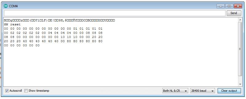
}
The program initializes the PCF8574 and writes 0xFF to D0..D7. The quasi-bidirectional lines are thus in a suitable state for use as an input. In the main loop (timed at 500mS) we perform a bus reading and then a HEX print of the read value. I made the complement because it is easier to understand 01 than FE ... In fact, using the test circuit proposed above and touching the various pins D0..D7 with the tip, we will have values such as 00 (the tip does not touch any pin) or 01, 02, 04, 08, 10, 20, 40, 80 touching from D0 to D7. Here's what we read on the serial monitor:
In this case, we can disconnect the red crocodile from the positive, while we will connect the black one to GND and close the jumper. We can also leave the red crocodile connected to +5; the voltage value on the input pin will be a little higher, but it should still be read as '0' when we touch the pins D0..D7 with the test lead.
Part 1 ends here. Part 2 will follow with the detail of the other output expansion, made with SPI bus, with the 74HC595A integrated circuit.
Emillotron - part 2
After the I2C device tests presented in Part 1, let's move on to the SPI I/O expansion device. It is a simple integrated 74HC595A. I've used it in the past to make a digital nixie tube clock (if you're interested, find it here: http://ficara.altervista.org/schemi.php#dg12h ) and it's very simple to use. It is a shift register with serial input and parallel / serial output and as many as you want can be connected in cascade. Here is the updated wiring diagram:
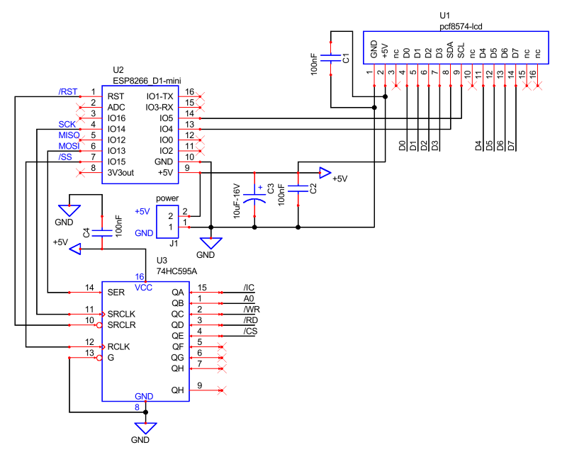
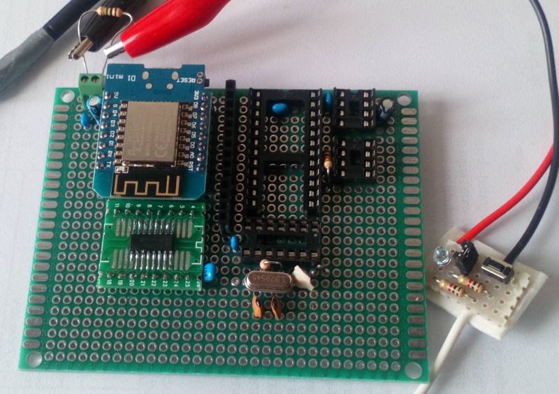
We see that the control signals for the Yamaha chip (/IC, A0, /WR, /RD, /CS) have been added which complete the series of connections together with D0..D7. We have 3 free bits on QF, QG and QH and they will probably be used going forward (for example, to drive an analog multiplexer). Obviously, to make things more complicated, I only had a few smd chips and so I had to use an adapter to mount the IC on the prototype board. Here's what came out:
The missing ICs are the main oscillator, the OPL-II chip, the DAC and an opamp. Note that the i2c module has also been removed for testing. For fun, we can also build a small resistive DAC, which will be useful for testing the shift register. The circuit is really elementary and is based on a resistive network in which each branch has double the value of the previous one:
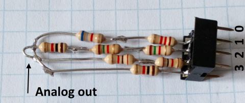
This is a 4-bit DAC, so we can have 16 analog levels, from 0 to 5V (supply voltage of the integrated HC595). Bit D3 has 1K resistor, D2 has 2K (1K + 1K), D1 has 4K (1K5 + 1K5 + 1K - I wanted to do 2.2K + 1.8K but I didn't have 1.8k-) and finally D0 has 8K (6.8 K + 1.2K). If we wanted to add a fifth bit (from the less significant side, shifting the other bits to the left) we would have to use a 16K.
Well, let's write a simple test program:
// Test SPI I/O expander (output mode)

#include <SPI.h> // this is for HC595

int LCK = 15; // GPIO15 - LCK (latch clock)
// note GPIO14 default SCLK \
// note GPIO13 default MOSI | ESP8266 in SPI mode
// note GPIO12 default MISO /

uint8_t wdata; // data write to shift register

void setup()
{
  delay(250); // power-on delay
  pinMode(LCK, OUTPUT); // set output mode for HC595 _/ LCK
  digitalWrite(SS, HIGH); // disable Slave Select
  SPI.beginTransaction (SPISettings (SPI_CLOCK_DIV64, MSBFIRST, SPI_MODE0));
  SPI.begin(); // begin with HC595
}

void loop()
{
  digitalWrite(SS, LOW); // low on latch clock
  SPI.transfer(wdata++); // send data and increment
  digitalWrite(SS, HIGH); // high on latch clock (rising edge latches)
  delay(5); // cycle time
}
Once the program has been transferred to the ESP8266 D1 mini module, we can go to measure the outputs of the shift register, with the usual led of the circuit shown in part 1, or we can use the resistive DAC by connecting it to the outputs QA, QB, QC and QD (where QA is bit 0). If we have an oscilloscope, we will see this:
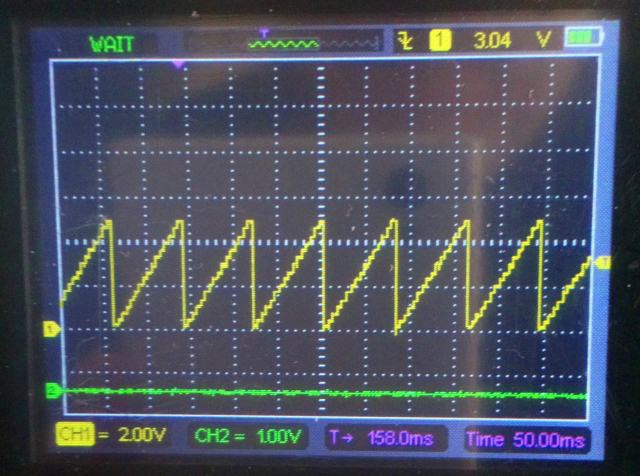
Our elementary DAC isn't perfect, but it's not bad! Keep in mind that it is NOT the one that connects to the OPL-II chip! This is only used to test the output lines of an HCmos logic. Part 2 ends here. We now have all the lines we need to drive the OPL-II chip and they seem to work. The next step will be to put everything together and try to write and read the internal registers, in order to generate the first sounds. Of course, to do this, we will also have to complete a minimum of analog part. The scheme of the "working base" will be presented in part 3 of the article.
Emillotron - part 3
Here is the new schematic diagram:
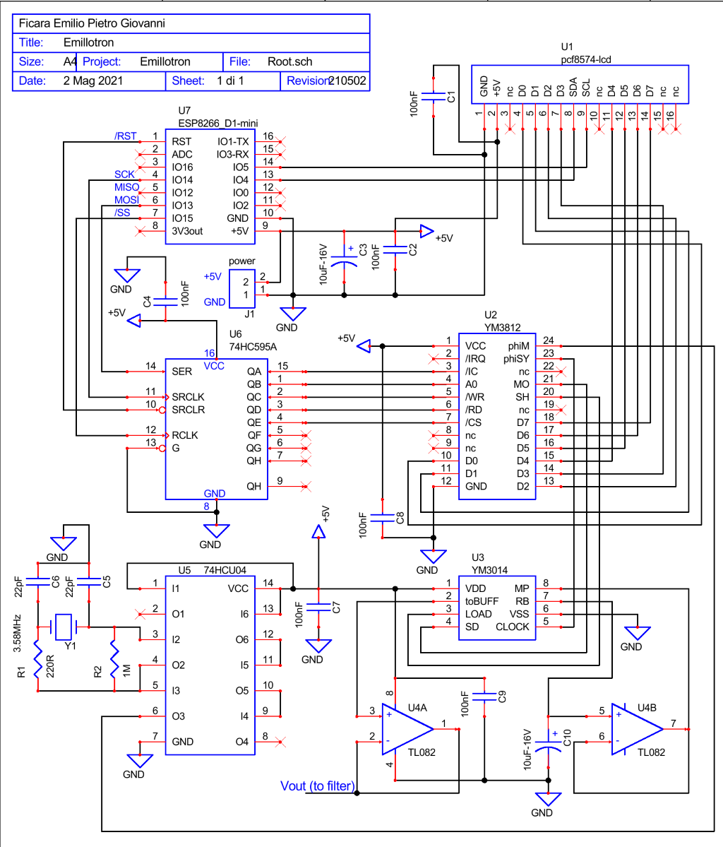
Please note: this is not the final diagram, since at the moment the power supply of the digital and analog parts are in common. At the appropriate time, there will be small changes to this section, in order to avoid hiss and hum on the low frequency. Also, you will need to add a low pass filter (another TL082) to the buffer output, before going to the audio output connector. For the moment, by connecting the output to an amplifier, you will be able to hear the effect of the writing of the various registers of the OPL-II chip (with some background noise). Here is also the complete realization of the prototype:
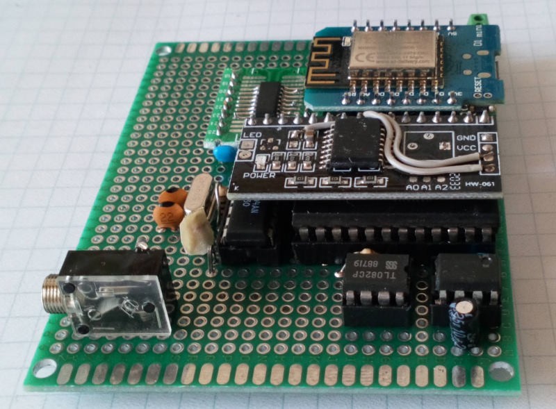
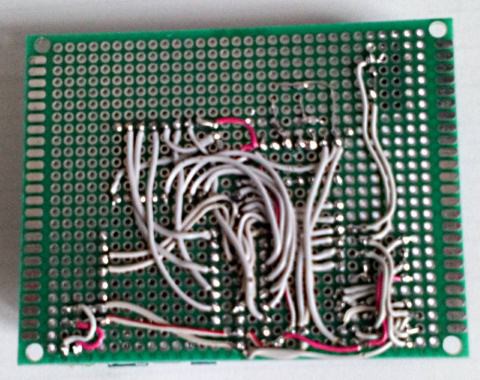
The OPL-II chip is hidden in the photo. If you look closely, you will see that it is under the I2C I/O expansion module. The quartz oscillator is made with a 74HCU04 (the U stands for “unbuffered”), but unfortunately I don't even have one of these chips, so I mounted a normal 74HC04 on the prototype. It oscillates the same, but for correctness, the one indicated on the diagram should be used. For those who love this type of "art", here is the circuit seen from the wiring side:
Let's start doing our tests. You can find in the "files" section the first version of the test program, named emillotron-v1.zip. The file is zipped with the password "eficara" and contains the working directory for Arduino. Let's see what's inside:
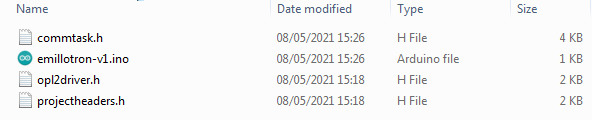
The commtask.h file (which is a C source anyway) contains the serial command parser. These are: +WR (write register) +RD (read status) +HR (hardware reset). The +RD and +HR commands are without parameters, while +WR requires the insertion of the register address and the value to be written to it, both in hexadecimal (all uppercase). The emillotron-v1.ino file is the “main” and contains the usual setup() and loop() functions. The opl2drive.h file is a C source which contains my basic functions for controlling the OPL-II chip (of course, based on the circuit described). Finally, the projectheaders.h file contains variables, constants, definitions, etc.
Through the serial monitor we can, after having compiled (for ESP826 D1 mini) and transferred the program to the module, give our commands. Each command starts with a + and ends with a CR (or LF). To verify, after the reset, that the card works, we try the command +RD and if we get in response 0x06, everything is fine and we can start the test to generate a sound.
This first version is very basic, but you can already do everything. Here is an example; we give below all these commands to obtain a timbre that I define as 'vocal':
+WR 20 01
+WR 23 82
+WR 40 30
+WR 43 0A
+WR 60 41
+WR 63 40
+WR 80 D4
+WR 83 D4
+WR C0 04
With these commands we loaded the parameters necessary to generate an FM sound in channel 1 (there are 9 channels).
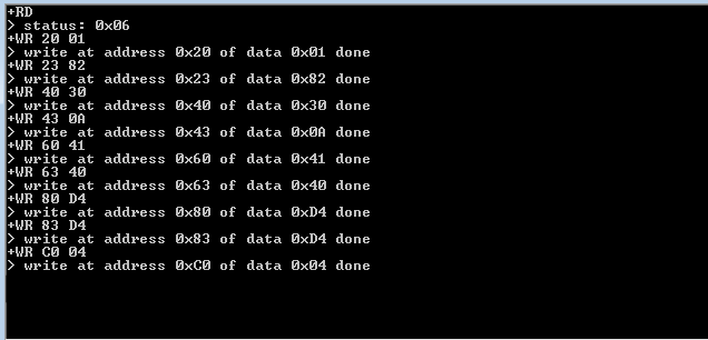
We can now try to "turn on" the sound, with a certain frequency. To do this, let's give a couple more commands:
+WR A0 07
+WR B0 2E
If the circuit is connected to an amplifier, we will hear the first sound. To stop it, we give the command:
+WR B0 00
Well, register A0 contains the low part (the 8 least significant bits) of the frequency divider; register B0 contains other 2 bits of the divider (the 2 most significant, there are ten in all) and then the block (the octave) and the note flag on. I recommend printing the component datasheet (YM3812) for an in-depth analysis of the registers. Let's try another timbre, which I call 'classic guitar':
+WR 20 23
+WR 23 21
+WR 40 25
+WR 43 0A
+WR 60 83
+WR 63 C2
+WR 80 F6
+WR 83 F6
+WR C0 0E

and now to play

+WR A0 07
+WR B0 2E

to stop

+WR B0 00
In the next part I will add: 1) hardware low pass filter and preamp; 2) software more complete set of commands to control the board in “easy” way. I will also add some 'presets' that come from my days in the music industry. This concludes part 3.
Emillotron - part 4
To go on with the rehearsals, I decided to build a musical keyboard with what I have at home (and by “home” I mean a temporary accommodation where I await the return to normal) to play without having to enter all the data by writing in the registers. Obviously, it is a very simple and mostly monophonic keyboard, so I can only play one note at a time. I thought about doing it like this:
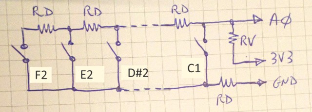
In my implementation there are 18 keys, from C1 to F2. In practice, each switch closes a series of resistors and through the ADC converter of the Esp8266 module we are able to obtain the pressed note. Here is the function that reads the keyboard:
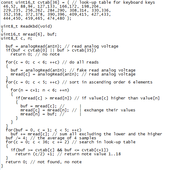
For stable reading, I used a technique that has already been useful to me on many occasions. In practice, the analog input is read for a certain number of times (six, in this case) and then the lowest and highest value are discarded and the arithmetic average of the remaining ones is calculated. I usually use a number of samples that is a multiple of 2, plus the two I'm going to discard. The reason for using a multiple of 2 is that then the division to obtain the average will be done with simple "shifts" to the right. In the table of CVTAB constants we find the values for converting the mean into a number from 1 to 18 (the keynote code, where 1 is the first Do (C1) and 18 is the last Fa (F2). The values are a pairs and indicate the minimum and maximum acceptable to say that the value read is relative to that note. I did some theoretical tests before, writing this little program in FreeBasic:
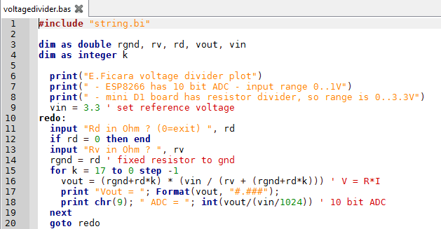
This is a screenshot of the resulting values, using 1KOhm for Rd and 22KOhm for Rv:
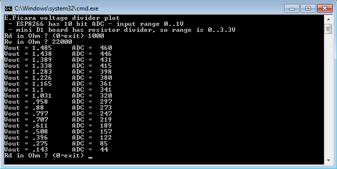
The actual values are slightly different from the theoretical ones, also because in fact the ADC converter of the ESP8266 has a range from 0 to 1V and therefore the manufacturers of the mini D1 module have inserted a resistive divider between pin A0 and the true input of the chip, in order to extend the input range up to 3.3V. The FreeBasic program does not take this additional element into account and then there are also the tolerances of the various components and the 3.3V power supply taken from the module to be considered. However, comparing the table with the theoretical values, we do not see a big deviation.
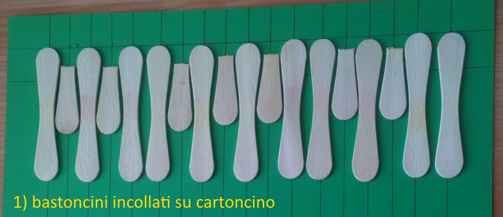
Here are the various stages of construction. As you will easily understand, I eat a lot of ice cream! The basic structure is made of a sturdy Bristol board with the "keys" glued on (with transparent double-sided tape):
Then you need the black keys and then, go with the permanent marker!

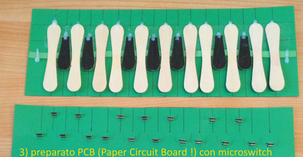
Now, using a part of the sheet, I made a kind of PCB (but it stands for "Paper Circuit Board") with extremely cheap microswitches that I had:
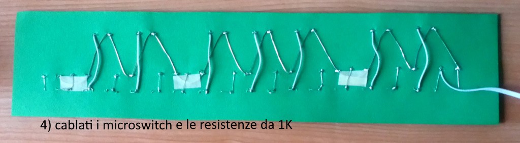
And then I wired the switches and resistors:
Here is the almost finished keyboard:
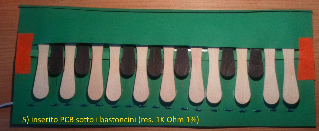
The resistances are still uncovered, so to finish the work, another nice round of orange tape!
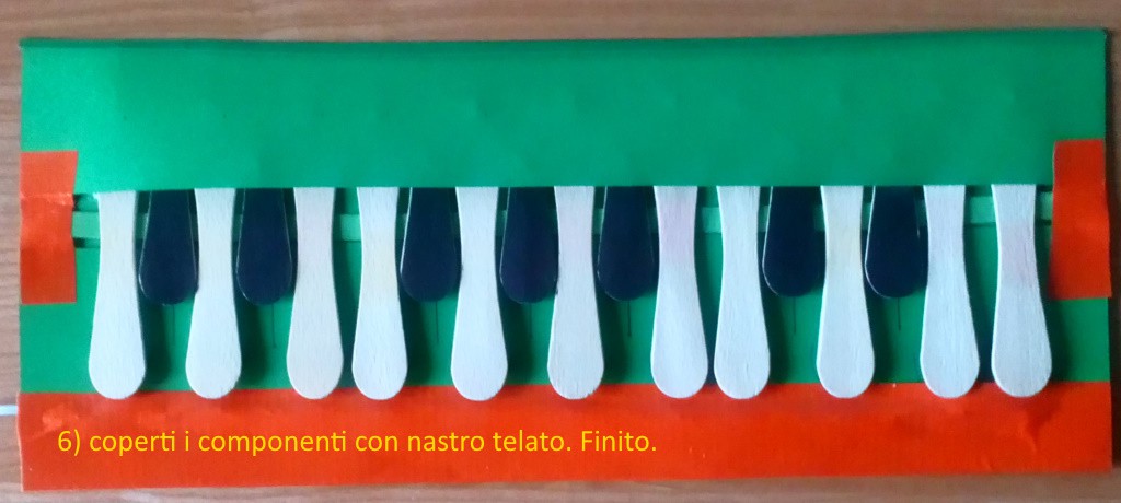
Here it is, in its splendor. Only two wires come out of the cardboard (left). If you measure the resistance between the ends with a tester, you will see a value in Ohms from 1K to 18K depending on the key pressed. The Rv is temporarily soldered under the prototype, between pin A0 and V3.3. The two ends of the keyboard are connected to GND and A0.
You will find the new firmware version (Arduino folder) in the “files” section, with name: emillotron-v2.zip and the password: eficara. In addition to reading the keyboard, I added a serial command and the note ON and note OFF functions. The serial command added is +LI n (with n ranging from 1 to 4). With this command you can load all the registers needed to generate a musical instrument all at once. The four instruments included are 1-Piano 2-Trumpet 3-Jazz guitar 4-Musette.
Obviously, once an instrument has been loaded, you can "play" with the registers using the serial command +WR rr dd and see what happens ... The keyboard, as we said, is monophonic and so if we press more than one key, the lower one will have priority (to the left). Note that up to this point, we have only worked on channel #1 of the nine available in the chip. We can, if desired, load a different instrument for each channel (just change the source a little) or make them all the same and thus have a polyphonic generator up to nine simultaneous notes. I invite you to look at my article mentioned by Hackaday at this link and specifically at this address on my site. Inside you will find the C sources to create a complete MIDI expander. Even if in the above example I used a PIC microcontroller to drive a sound card on the ISA bus, the functions are identical! The only thing that changes is the management of low-level writes. For those, you have to use the new C functions attached to this article.
In the next part (the fifth and last) I will publish the new scheme with the small changes related to the power supply of the analog part and to the filter / preamp in output. In the meantime, have fun!
Emillotron - part 5
Here we are at the end of this experiment. From this base I will build my generator of casual and relaxing melodies, probably using the algorithm described in my previous article on "musical" artificial intelligence (AmI, see my other projects here).
Here is the updated schematic:
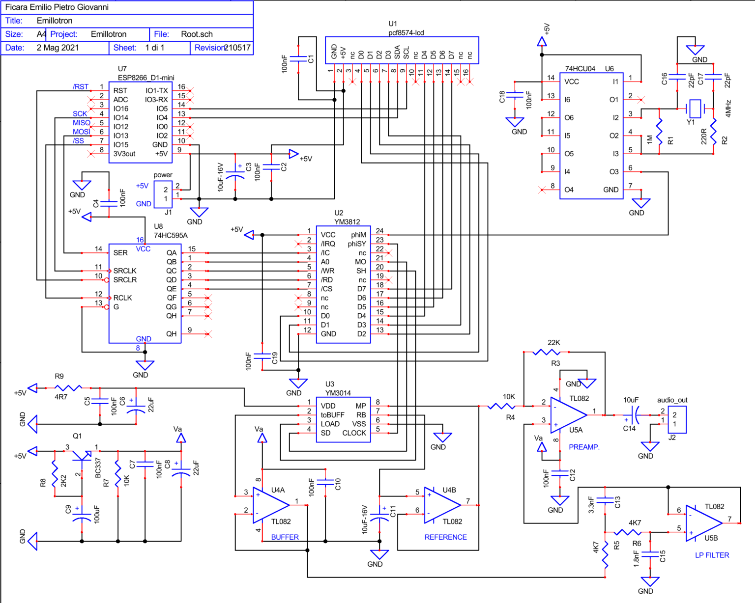
As you can see, I added filters on the power supply, in addition to the audio low-pass filter and the output preamp. Powering everything with the 5V of the USB, the result is pretty good, especially considering how “dirty” the 5V power supply coming from a PC or a telephone battery charger is normally. Another note: I changed the quartz, taking it from the original 3.58MHz to 4MHz. The reason is simple: I need 3.58 for another project and I only have one! Of 4MHz, however, I have several. No worries: the tables to generate the notes are adapted to this quartz frequency (even in the previous firmware). The 4.7Ohm resistor that acts as a filter to the DAC does not cause a large voltage drop. On the datasheet it says that the maximum absorption of the DAC is 6mA, therefore the maximum drop is about 0.03V, very acceptable.
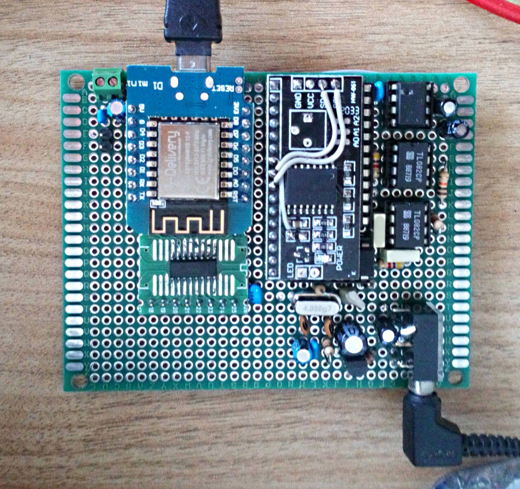
Here is the updated prototype:
I conclude here and I hope that my work will be useful to those who love to build things with their own hands. See you at the next project, bye.