 kaimac
Thinking about timing and whether I'm happy with this aspect of the design.
Each instruction consists of some number of operations (phases? cycles?), where the 24 control lines are set appropriately. That information is held in a control store of 3 64Kx8 EEPROMs, which are addressed by the 8-bit instruction register, a 4-bit sequence counter, and the three status flags (for conditional jumps).
Here's an example of how an instruction is defined:
add x, #L
    pcinc memrd twr                         ;write literal to T
    regoe alu opadd regwr selx setflags     ;X = ALU(X, T, op=add, setflags=yes)
    pcinc memrd irwr                        ;write next opcode into IR (fetch - common to all instructions)
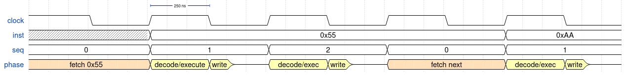
So far I've been thinking of the timing like this:
- On the clock's rising edge, clock the program counter, instruction register and sequence counter.
- During the high half of the clock, instruction decoding and execution (i.e. ALU computation) is underway.
- On the clock's falling edge (rising edge of ¬CLK), write back any values to registers, or to memory.
While this has its problems, it seems to be a popular method with simple homebrew CPUs. For example the very well documented CSCvon8: An 8-bit TTL CPU and the SPAM-1 - 8 Bit CPU.
Interestingly, many people describe this as "fetch/decode" on the high part of the clock, and "execute" on the low part. Is that correct? Maybe you can argue either way, but to me it makes sense to consider the time it takes for the ALU to produce a valid result as execution time, just as decoding is what is happening while the control store ROMs are producing a valid output. Writing back values to RAM or to registers takes little time in comparison (in the case of registers, no time at all).
And that's one of this method's weaknesses - pretty much everything happens during only one half of the clock cycle, limiting performance. In my case, it looks like 2 MHz will be the maximum clock rate.
A design where things only happen on the clock's rising edge would be more pleasing to me - and more performant. But for the sake of simplicity I'll probably keep it the way it is. Things can always be improved in the next design!
Discussions
Become a Hackaday.io Member
Create an account to leave a comment. Already have an account? Log In.
I got at least 3.4mhz on SPAM-1 on breadboard and that's with a square wave clock. I've considered making the execute phase shorter by using a asymmetric clock. Since SPAM-1's critical path is the time taken for the program ROM to settle and the ALU ROM to settle during the fetch/decode and the execute phase is just registers and a fast RAM then I'd get perhaps a 25% - 40% savings on cycle time meaning perhaps another MHz or so but the signal propagation problems on breadboards and long wires might start to kick in at that point.
In the end even if you were to do it all on one clock edge, the clock still has to return to the other phase, can't avoid two edges. I asked a more general question which was what do folk mean by "single cycle CPU" , at one point like you I wondered about single-edge but generally folk mean just what it sounds like "useful work done in a single cycle". So for inst6if microcoded CPUs can't do useful work in a single cycle then I guess they aren't single cycle CPUs.
In spam-1 my program ROMs are ffash and fairly fast but its the ALU that is the limiting factor. But let's say you had slow program ROMs and also ALU then it pays off to separate fetch and decode into two concurrent activities using pipelining perhaps.
Another consideration is that spam-1 is Harvard and that matters because it means the CPU can access the program memory and the data memory in the same cycle because there are distinct address paths for the program and data memory. In a Von-Neuman most would load from ROM to RAM via a register. There might be other interesting diffs between Harvard and VN that you should consider.
My next CPU will be a modified VN that has some of the benefit of Harvard with the flexibility of VN.
Are you sure? yes | no