 lion mclionhead
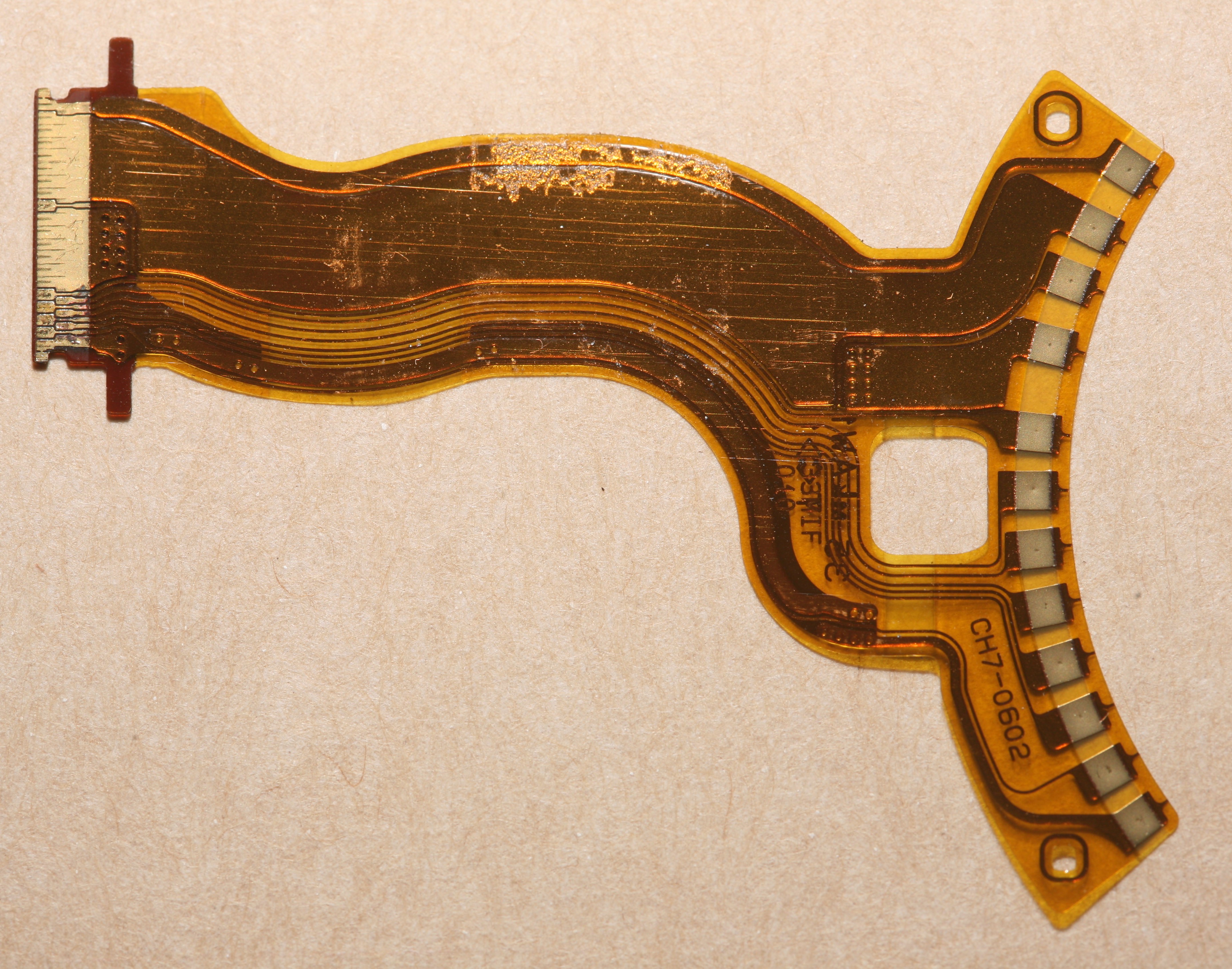
It might have been Dave Jones or Louis Rossmann, but there was a rumor about a guy who photographed a cable & instantly got a gerber file out of it for a new cable. It's not that easy. There's parallax distortion in a photo. The edges aren't exact. There might be a way with a flatbed scanner & manually tracing outlines.
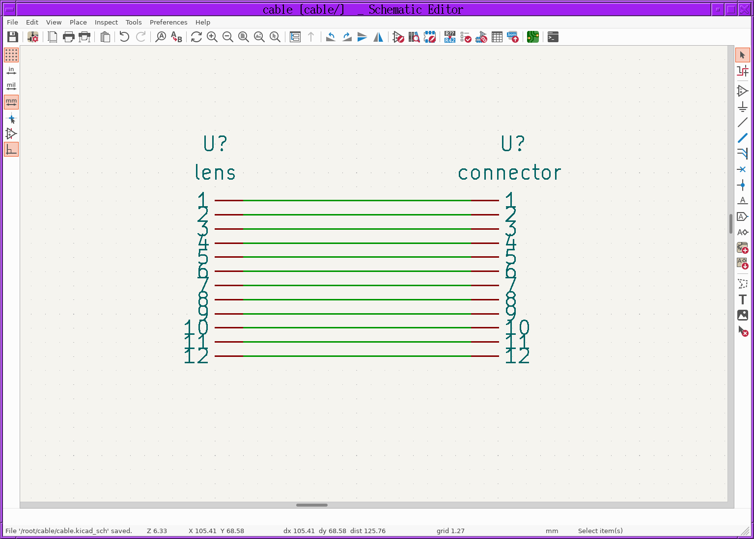
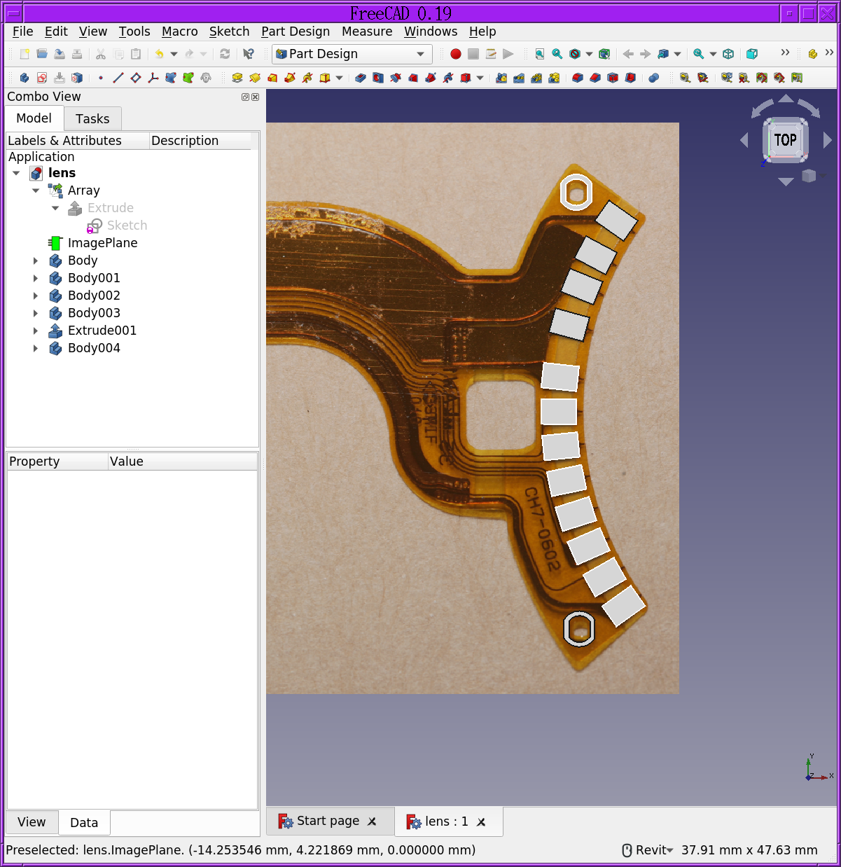
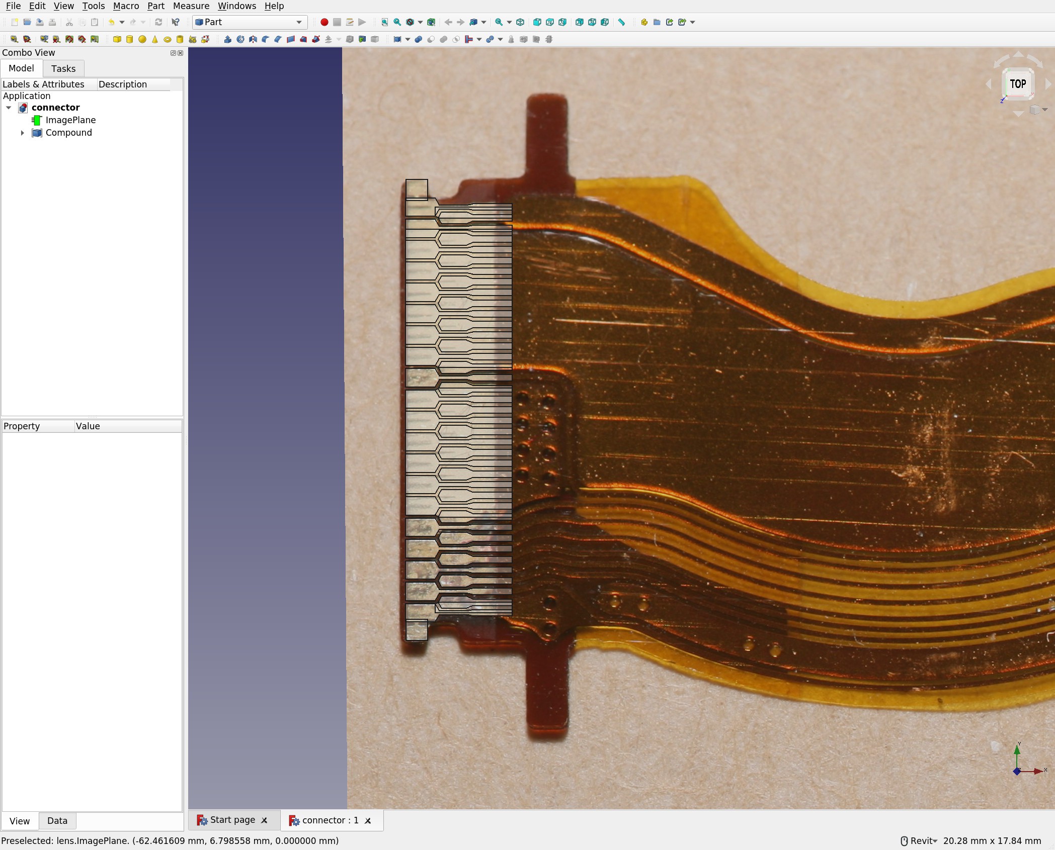
The lion kingdom wanted to migrate to kicad, which further complicated matters. The journey begins by creating lens & connector symbols.
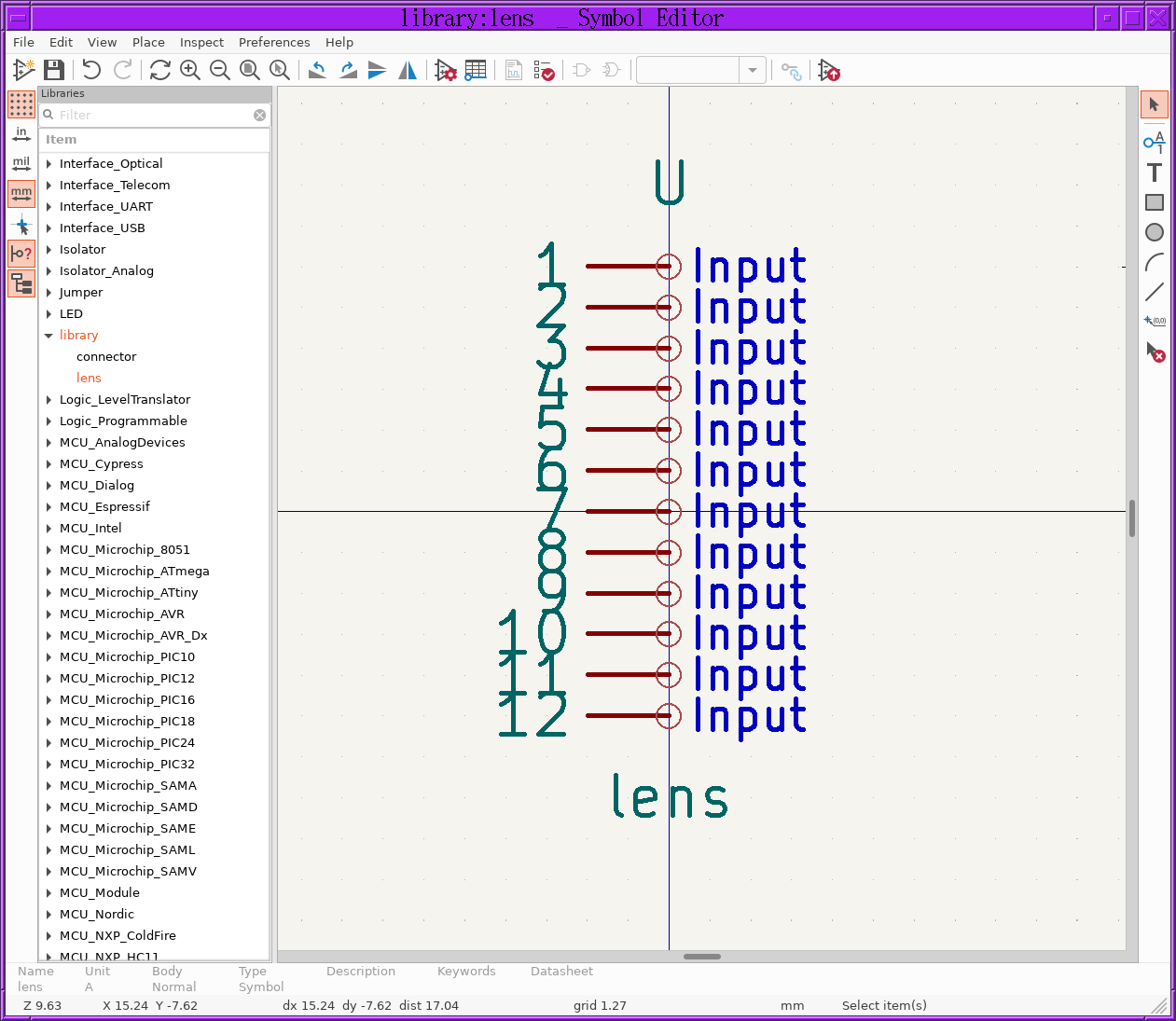
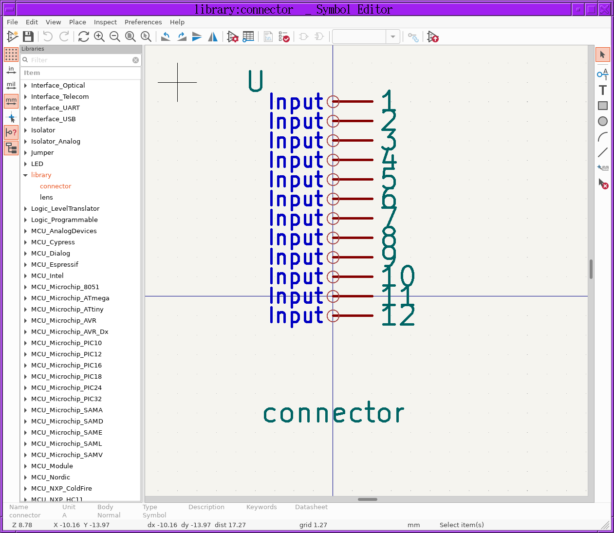
Then creating a schematic connecting the symbols.
The trick is creating the footprints. The Kicad footprint editor has simple freepaw polygons, an ortho array tool, but no history. Supposedly, animals manually draw every pad, using the grid & ruler tools. Lions made all their footprints for geda-pcb in a text editor just to get reproducible dimensions. Freecad has constraints, polar arrays, mirrors & history. There's a tool in the Image toolbox to scale the image to mm.
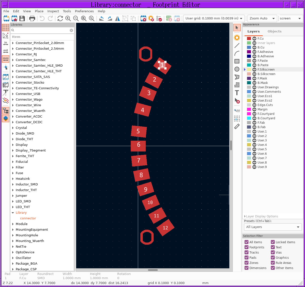
There is a way to draft the pads in freecad, save it as a PNG file, & import the bitmap into kicad as a silk screen. It requires having the footprint editor & image converter side by side. Create a new library & footprint in the footprint editor. Load the image in the image converter. Export the image to the clipboard. Paste the clipboard in the footprint editor.
The only way to scale the image in kicad is calculating pixels/mm in a spreadsheet. To transfer it to a copper layer, you have to edit the footprint in a text editor. Then add pads on top of the drafted pads to assign them to pin numbers. The lion kingdom ended up using a text editor to change the pad sizes.
That might have been easier by manually tracing the footprints instead of using the array tool.
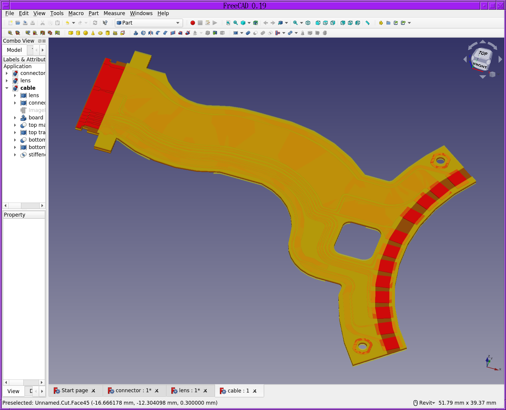
This was made of an array of dummy pads of sensible dimensions. The photo was rotated & scaled until the dimensions agreed with what the calipers saw & reasonable pad dimensions. Then polygons were added to join the pads. The pads ended up being .5mm spacing with .07mm gaps.
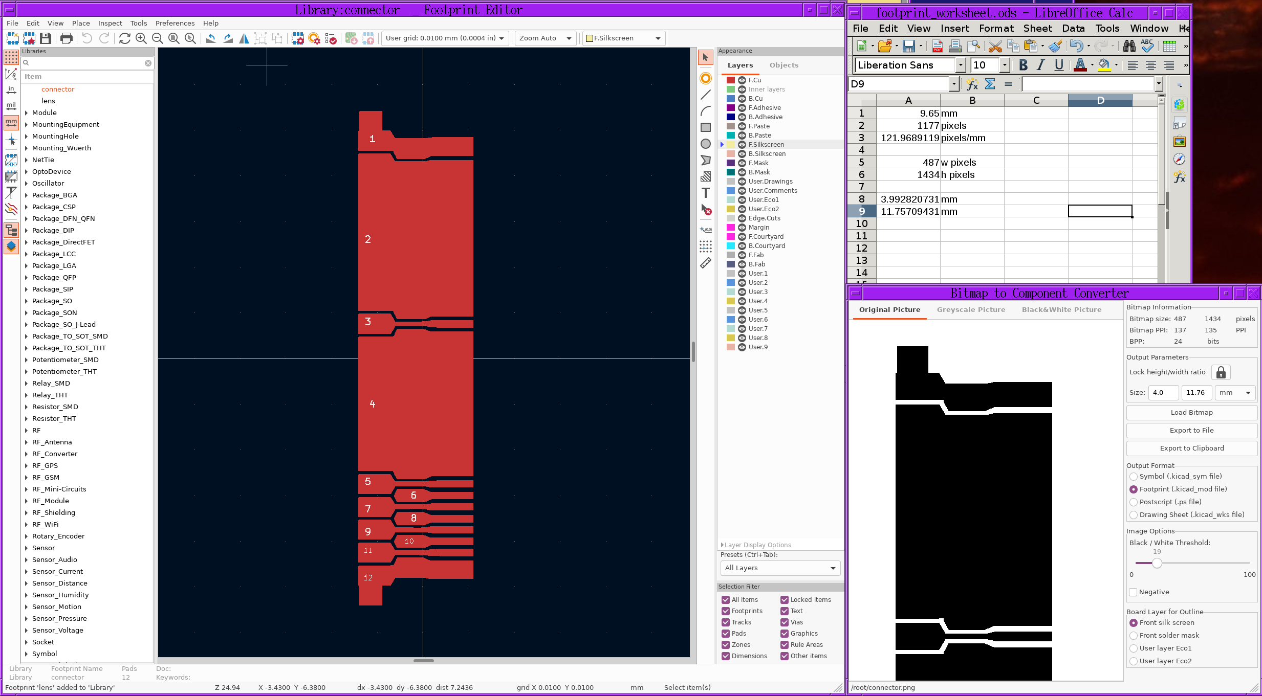
We have the footprint spreadsheet, bitmap converter, & footprint editor on 1 of many iterations of the footprint.
With the board layout, we have the problem of polygons made of parametric curves. Kicad can only make simple freepaw polygons out of straight lines so attention turned to freecad.
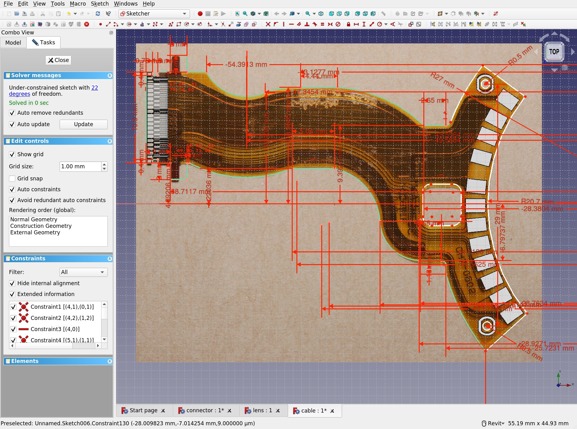
The fact that the lock tool puts the numbers 10mm away from the polygon while the horizontal & vertical contraint tools put the numbers in a sensible place is a serious bug.
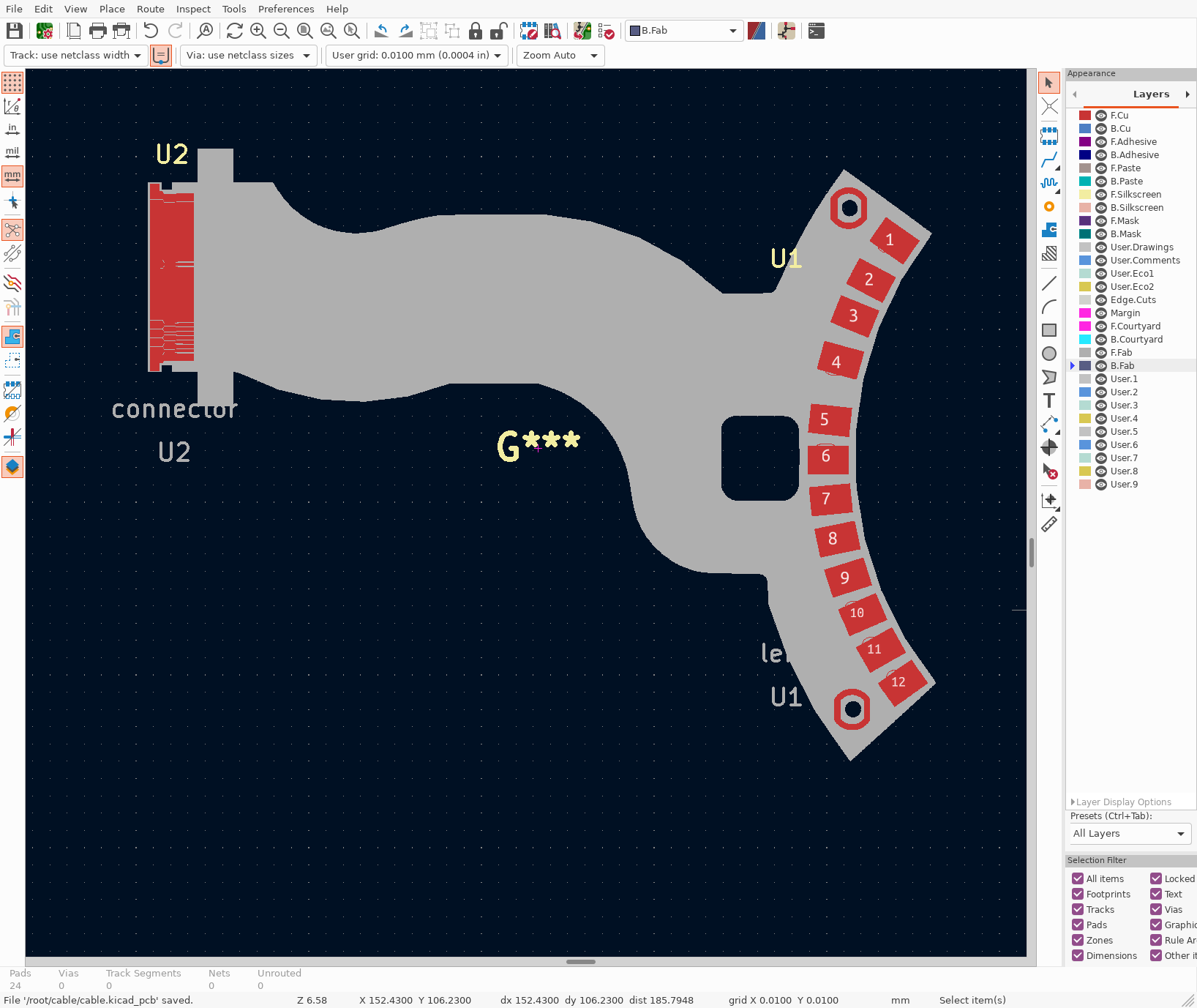
Once again, the photo dimensions were slightly off of the caliper dimensions, so merely tracing the photo wouldn't work. The same routine of capturing PNG screenshots, loading into kicad's bitmap converter, computing sizes in mm, copying to the clipboard, pasting into the PCB editor, changing the layer in a text editor, yielded the board outline.
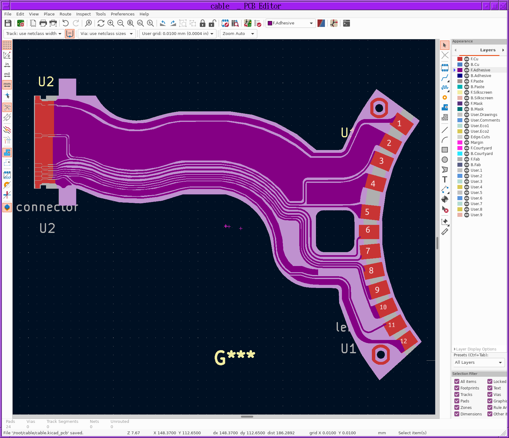
Eventually kicad fell over after importing a trace layer. The navigation just isn't up to editing such a complicated nest of fine pitched, curved traces. The text boxes in the image converter just aren't accurate enough. There's no way to directly enter the DPI. It tries to vectorize the bitmaps, which adds more error. It has the usual newby mistakes when programming an object oriented drawing program, differentiating between zoom & translation, differentiating between grab & move, unreliable selections, text boxes which don't immediately update the layout. It can't flip the board over & view from the back. It only brings the active layer to the front.
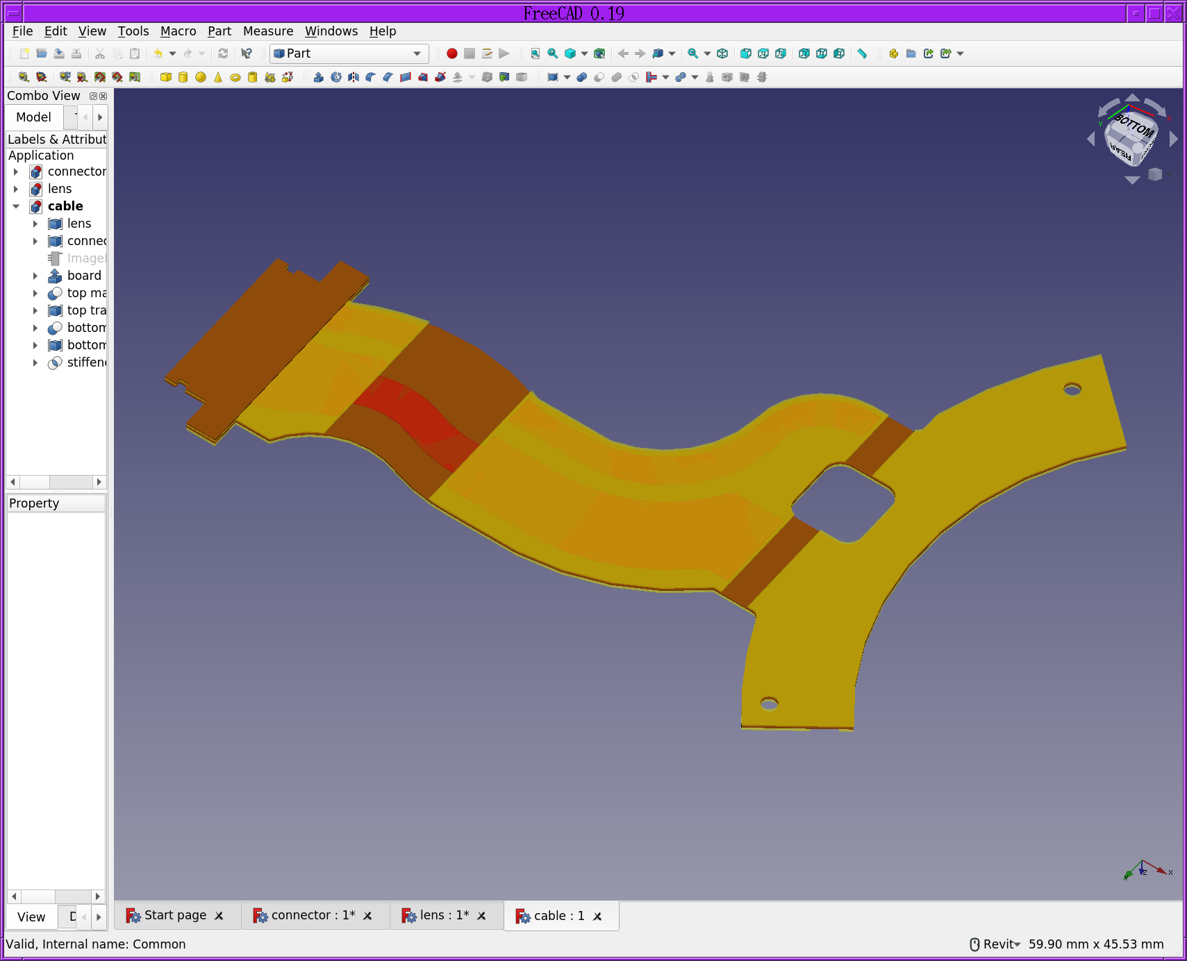
The board except for the drill holes was easier to fully model in Freecad. What's needed is a way to directly export gerber files & drill files from Freecad. The leading idea is exporting every layer as an image of equal resolution & translation, importing them all into kicad with the same DPI, not using discrete footprints since there's no way they'll line up. Kicad doesn't have a way to import existing layouts into a layout like geda did. There's just editing the kicad_pcb file directly. You can create a fp_poly block with a vectorized footprint. It may just require Eagle or Altium.
Discussions
Become a Hackaday.io Member
Create an account to leave a comment. Already have an account? Log In.