Fortunately most of the NASA documents are available. They can be found on-line at https://www.ibiblio.org/apollo/Documents/
The following documents are what I leaned heavily on in gaining an understanding of how this computer works.
R-393.pdf → Logical Description for the Apollo Guidance Computer (AGC4)
E-2052.pdf → AGC4 Basic Training Manual
1689.pdf → AGC4 Memo #9 – Block II Instructions
R-700.pdf → Computer Subsystem
AGC Information Series, ISSUE 32 Block II Machine Instructions
That last document is the most important. Without it I would have been guessing. That document shows each instruction and the control pulses required to execute the instruction. The control pulses are stored in a Control Pulse Matrix. There are a few slight errors in the CPM laid out in this document, but I found the correct version in other documents. The original CPM was created using a matrix of diodes. I chose a simpler, more modern method, burn the information into an EPROM.
In the original R-393 document, Chapter 2 describes blocks of functionality diagramed in Figure 2-1. I have choose to refer to these blocks as modules. There are 17 modules described below; 15 from the original documentation and an additional module used to monitor and debug the hardware plus I added a pseudo module to describe the Channels. In the implementation, there is no Channel module as this functionality is parsed out into other modules. The modules are as follows:
- Clock
- Scalar
- Central Registers
- Arithmetic Logic Unit
- Sequence Generator
- Timing Pulse Generator
- Control Pulse Matrix
- Interrupts
- Counters
- Memory Address
- Memory Buffer
- Erasable/Fixed Memory
- Parity Generator
- Keyboard
- Display
- Channels
- Monitor
Data Format: A computer word is 16 bits in length. The math is primarily 1's compliment arithmetic. The instruction word consists of a 3 bit opcode, 12 bit operand and 1 parity bit. The single parity bit exists to detect single bit memory errors. The data word is similar in that it consists of 14 bits of data, and two sign bits.
When data is moved from memory into a central register, the parity is automatically checked and then the parity bit is replaced by a sign bit, so a central register word consists of the same 14 bits of data and two sign bits. The sign bits decode as follows.
| Bit16 | Bit15 | Meaning |
|---|---|---|
| 0 | 0 | Positive |
| 1 | 1 | Negative |
| 0 | 1 | + Overflow |
| 1 | 0 | - Overflow |
Block II introduced the concept of double precision numbers. This is why the L register was moved next to the A register so the two registers together can make up a double precision number. With A being the more significant number and L being the lower. The format for a double precision fraction is +/- A * +/- 2 ** B where the sign of A is the overall sign of the number and the sign of B is the sign of the exponent.
Buses: In Block I there was a read bus and a write bus. This was a strange concept that did not survive in Block II. The newer documentation refers to the single data bus as the write bus. There are also added buses that move data directly from the A to X register and between the L and G registers. These two buses facilitate some of the time reduction of the multiply and divide commands. The Channel Bus was added in Block II to free up erasable memory.
The Clock (CLK) module is simply a 4 MHz crystal that provides the heartbeat of the system. This module divides the 4 mHz pulse by four to produce four non-overlapping 1 MHz clock signals. The clock signals are used to trigger various internal operations. The reason for more than one clock signal is that if you simultaneously assert the RA and WB control pulses to move data from the A to B registers you will not get consistent results. The data must be on the write bus before the WB pulse latches the data. Both control pulses are asserted simultaneously, however you must first assert the RA control pulse to place the data onto the write bus, then a short time later assert the WB control pulse. This is accomplished by ANDing the RA pulse with the first control signal and ANDing the WB pulse with a second control signal that follows a short time later.
The Scaler (SCL) module divides the clock in half 17 times to give progressively slower clock pulses. This provides hardware driven periodic timers that drive various elements of the system. First the clock is divided by two to produce a Master Frequency of 512 kHz. This value is divided by 5 to produce a 102.4 kHz frequency, then by 2 successively 17 times. The available scaler values are as follows.
| Scalar | Seconds | Hertz |
|---|---|---|
| Clock | 0.000001 | 1,024,000 |
| MFreq | 0.000002 | 512,000 |
| . | 0.0000098 | 102,400 |
| F1 | 0.0000195 | 51,200 |
| F2 | 0.000039 | 25,600 |
| F3 | 0.000078 | 12,800 |
| F4 | 0.000156 | 6,400 |
| F5 | 0.000315 | 3,200 |
| F6 | 0.000625 | 1,600 |
| F7 | 0.00125 | 800 |
| F8 | 0.0025 | 400 |
| F9 | 0.005 | 200 |
| F10 | 0.01 | 100 |
| F11 | 0.02 | 50 |
| F12 | 0.04 | 25 |
| F13 | 0.08 | 12.5 |
| F14 | 0.16 | 6.25 |
| F15 | 0.32 | 3.125 |
| F16 | 0.64 | 1.5625 |
| F17 | 1.28 | 0.78125 |
System time is generated using a pair of counters fed by the 10 milli-second clock pulse. The pair of counters that make up system time are named Time1 and Time2, the same as in Block I. The Time1 counter is fed by the 10 mSec clock pulse. This counter counts up to 163.84 seconds and the overflow feeds the Time2 counter which counts up to 30 days. Thirty days was more than enough time for an Apollo mission to the moon.
There is also a more accurate timer introduced in Block II that consists of a pair of channel registers. The more accurate timer consists of Channel 4 which is fed by the F5 3.2KHz clock pulse that counts up to 5.12 seconds. The overflow of Channel 4 feeds Channel 3 which counts up to 23 hours.
The Central Registers (CRG) module consist of the Accumulator (A) register, the Lower Accumulator (L) register, the Program Counter (Z) register and the Return Address (Q) register. These registers are controlled by two control pulses each; a read and a write pulse. The A and L registers have special write control pulses that can shift bits right by one. Block II added a feature where the A register data can be written directly to the X register, bypassing the write bus. The L register data can also be exchanged with the G register directly.
This module contains a portion of the channel implementation since channel data is read from and written to the A register. The channel portion implemented here is the AND, OR and XOR of the A register with the channel data.
The central registers are physical registers that have addresses in the erasable memory address range. There are three additional Special registers that relate to memory management. These are the EB, FB and BB registers. The seventh register is all zeros as many computer functions require a zero constant. Together these seven registers make up the “Central Registers”. The following are the registers and their addresses.
00 = A register : Accumulator
01 = L register : Lower Accumulator
02 = Q register : Return Address
03 = EB register : Erasable Bank
04 = FB register : Fixed Bank
05 = Z register : Program Counter
06 = BB register : Both Banks
07 = Zeros : All zeros
The control pulses are relatively straight forward. For example, data is written to the A register using the WA control pulse and read using the RA control pulse. There is a special WALS control pulse that writes to the A register, shifting right two bits. Bits 1 and 2 are written to bits 13 and 14 of the L register. The results are shown below where B1-B14 are the bits as read from the write bus, D0 means set the bit to zero, SG means the sign bit, US means the uncorrected sign bit.
A reg: SG,SG,SG,US,B14,B13,B12,B11,B10,B9,B8,B7,B6,B5,B4,B3
L reg: D0,D0,B2,B1,D0,D0,D0,D0,D0,D0,D0,D0,D0,D0,D0,D0
The Arithmetic Logic Unit (ALU) module consists of the general purpose B register and the X and Y registers that are added together with the results placed into the U register. The ALU also performs a 1’s compliment on the B register (referred to as the C register). The U register can be added to the B register. The B register has a number of purposes, however its main purpose is to store the next instruction.
The ALU can set frequently used constants onto the write bus. The constants include the following control pulses and the resulting octal value that is OR'ed onto the write bus.
R15: 000015
R1C: 177776 (-1)
R6: 000006
RB1: 000001
RB1F: 000001 if BR1=1
RB2: 000002
RSTRT: 004000 (start program address)
There is a direct connection between the A register and the X register controlled by the A2X control pulse. There is also a direct connection between the G register and the L register controlled by the L2GD and G2LS control pulses. These links did not exist in Block I.
The WX and WY control pulses write data from the write bus into the corresponding registers. The RU control pulse reads the output of the resulting U register. There is a CI control pulse that forces a carry-in bit and therefore adds one to the result. Data can be written to the B register with the WB control pulse. The resulting data can be read using the RB control pulse or the 1's complement of the B register is read using the RC control pulse.
The Block I design performed multiplies by adding and shifting 14 times, once for each bit of the multiplier operand. Two additions occurred per memory cycle time (MCT), resulting in 8 MCTs plus the 2 MCTs for the extend operation for a total of 10 memory cycles to perform a multiply.
In Block II the design was modified to increase the speed of a multiply. This was accomplished using a carry skip, using two multiply bits at once and dedicated wire word transfers. The result is a total of 3 MCTs, a reduction of 7 MCTs.
The first logic change is the carry skip which decreases the worst case propagation delay by anticipating a carry out of the next four successive stages. “Carry-prone means that one or both operand bits are 1. When a group of successive stages are carry-prone and a carry enters the lowest order of the group, there is necessarily a carry out of the highest order stage of the group.” This means that the sum can be read at the pulse time following the addition.
The second logic change is dealing with two multiply bits at once. The multiplicand is added 0, 1, 2, or 3 times to the partial product. The multiply by 0 and 1 cases are performed by either suppressing or allowing the addition of the multiplicand. This is the same as with the Block I multiply. The multiply by 2 case is performed by adding the multiplicand shifted left one position. This requires a special write gate on the Y register. The multiply by 3 case is more complicated in that it is accomplished by multiplying by 4 and subtracting once. The multiplicand is first subtracted and you have to remember to add a 1-greater multiple during the next addition cycle. This addition during the next cycle is a multiply by four using a 2 bit shift. Subtraction is handled by storing the multiplicand in the B register, giving the 1's compliment in the C register.
The third logic change is dedicated wiring that was added between the A and X registers and between the L and G registers to allow simultaneously loading of the X and Y registers and simultaneously shifting of the A and L registers.
The divide instruction was reduced from 18 to 8 MCTs due to the faster adder and dedicated transfers. Block II removed the carry prolongations in the adder. The carry anticipation circuit suppresses every fourth existing carry resulting in carry propagation within one pulse time.
Multiplication multiplies the multiplier and the multiplicand to get the product. The AGC multiplies the single precision value in the A register with the value defined by “K” (the operand). The resulting double precision product is placed in the A,L register pair (A is the more significant word). The sign of the product is positive if the signs of the multiplier and multiplicand are the same. The sign is negative if the two have different signs.
Division divides a dividend by a divisor to get a quotient. The AGC places a double precision dividend into the A,L register pair (A is the more significant word). The divisor is defined by “K” (the operand). The resulting quotient is deposited in the A register and the remainder is in the L register. The sign of the quotient (A) is positive if the signs of the dividend and divisor are the same, negative if different. The sign of the remainder (L) is the sign of the dividend.
The Sequence Generator (SEQ) module keeps track of the current instruction being executed in the SQ register and extend bit along with whether a branch is being performed and the staging control. If more than one MCT is required, the stage counter is incremented. The stage register was increased to three bits in Block II to accommodate the new divide instruction. The branch register is two bits. There are various control pulses that drive the sequence generator.
Given an opcode of three bits, only 8 instructions are possible. This is too limiting, even for the Block I version. The number of instructions is increased by using two methods; extension and quarter codes. Extension is where the EXTEND instruction precedes the instruction to extend. This is used for the less frequently used instructions because it requires an additional MCT. Extension is used to double the number of instructions. The extend bit is bit 16 of the SQ register which replaces the parity bit once the instruction has been read from memory. This trick was used to get to the required 11 Block I instructions.
Block II introduced the concept of quarter code instructions whereby the opcode encroaches on the operand or address field by two bits. Less than 12 bits are required to define erasable memory and channel addresses, therefore the instructions that do not operate on fixed memory addresses can be combined, each being assigned a quarter code.
The following table shows a simplified view of the commands. The opcodes can have a value of 0 through 7. The quarter code field designated QC extends the opcode field. The highest order 2 bits of the operand is the QC field. The Extracodes are instructions that are preceded by an EXTEND instruction which sets the extend bit (bit 16). If the extend bit is set and the opcode is zero then the instruction is a channel instruction. The channel instruction is determined by the highest order 3 bits of the operand field designated as PC. There are a total of eight channel instructions.
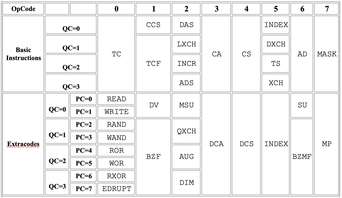
Another way to look at this is how the three types of instructions overlap. Regular or general instructions are determined by the contents of bits 16 - 13 of the SQ register. Regular instructions with quarter codes or erasable memory instructions are defined by bits 16 - 11. The channel opcodes use bits 16 - 10 of the SQ register. For the channel instructions, the extend bit is always set.
Regular Instruction: Extend bit (16) : Opcode (15-13) : Operand (12-1)
Quarter Code Instr: Extend bit (16) : Opcode (15-11) : Operand (10-1)
Channel Instruction: Extend Bit (16) : Opcode (15-10) : Operand (9-1)
The current instruction is kept in the SQ register. The following table lists each basic instruction, its opcode (theSQ register value), memory usage and description. 'x' means the bit is ignored during instruction decoding. Note that bit 16 of SQ is the extend bit which replaces the memory parity bit. The “All” memory designator means that all memory can be addressed using this command. The “Erasable” memory designator means that only erasable memory can be addressed using this command. The “Fixed” memory designator means that only fixed memory is addressed using this command. The “Channel” memory designator uses a special channel number instead of an address. Bit 10 is only used for the channel command. Bits 15-13 are the opcode. Bits 12-11 are the quarter codes.
| Code | SQ Reg (16 - 10) | Memory | Description |
|---|---|---|---|
| TC | 0 0 0 0 x x x | All | Transfer Control w/ Return Address |
| CCS | 0 0 0 1 0 0 x | Erasable | Count, Compare and Skip |
| TCF | 0 0 0 1 [1-3] x | Fixed | Transfer Control to Fixed F |
| DAS | 0 0 1 0 0 0 x | Erasable | Double Add A & L to Storage E,E+1 |
| LXCH | 0 0 1 0 0 1 x | Erasable | Exchange L with Storage E |
| INCR | 0 0 1 0 1 0 x | Erasable | Add 1 to Storage E |
| ADS | 0 0 1 0 1 1 x | Erasable | Add A to Storage E |
| CA | 0 0 1 1 x x x | All | Clear & Add K to A |
| CS | 0 1 0 0 x x x | All | Clear & Subtract K to A |
| NDX | 0 1 0 1 0 0 x | Erasable | Index Next Basic Instruction |
| DXCH | 0 1 0 1 0 1 x | Erasable | Double Exchange A & L with Storage E,E+1 |
| TS | 0 1 0 1 1 0 x | Erasable | Transfer to Storage E |
| XCH | 0 1 0 1 1 1 x | Erasable | Exchange A with Storage E |
| AD | 0 1 1 0 x x x | All | Add K to A |
| MSK | 0 1 1 1 x x x | All | Bitwise AND of A with K |
| DV | 1 0 0 1 0 0 x | Erasable | Divide A & L by Storage E to A |
| BZF | 1 0 0 1 [1-3] x | Fixed | Branch on Zero to Fixed |
| MSU | 1 0 1 0 0 0 x | Erasable | Modular Subtract from A |
| QXCH | 1 0 1 0 0 1 x | Erasable | Exchange Q with Storage E |
| AUG | 1 0 1 0 1 0 x | Erasable | Increase Abs Value of Storage E by 1 |
| DIM | 1 0 1 0 1 1 x | Erasable | Decrease Abs Value of Storage E by 1 |
| DCA | 1 0 1 1 x x x | All | Double Clear & Add K,K+1 to A & L |
| DCS | 1 1 0 0 x x x | All | Double Clear & Subtract K,K+1 from A & L |
| NDXX | 1 1 0 1 x x x | All | Index Next Extra-Code Instruction |
| SU | 1 1 1 0 0 0 x | Erasable | Subtract E from A |
| BZMF | 1 1 1 0 [1-3] x | Fixed | Branch on Zero or Minus to Fixed |
| MP | 1 1 1 1 x x x | All | Multiply K by A, store into A & L |
| Channel Instructions: | |||
| READ | 1 0 0 0 0 0 0 | Channel | Read from Channel to A |
| WRITE | 1 0 0 0 0 0 1 | Channel | Write A to Channel |
| RAND | 1 0 0 0 0 1 0 | Channel | Read Channel to A (ANDed with A) |
| WAND | 1 0 0 0 0 1 1 | Channel | Write to Channel (ANDed with A) |
| ROR | 1 0 0 0 1 0 0 | Channel | Read Channel (ORed with A) |
| WOR | 1 0 0 0 1 0 1 | Channel | Write to Channel (ORed with A) |
| RXOR | 1 0 0 0 1 1 0 | Channel | Read Channel (XORed with A) |
| EDRUPT | 1 0 0 0 1 1 1 | Channel | Force Interrupt (not implemented) |
| Special Instructions: | |||
| RUPT | 1 0 0 0 1 1 1 | n/a | Interrupt Processing |
| EXTEND | 0 0 0 0 1 1 0 | n/a | Extend instruction (K = 06) |
| INHINT | 0 0 0 0 1 0 0 | n/a | Inhibit interrupts (K = 04) |
| RELINT | 0 0 0 0 0 1 1 | n/a | Release inhibit interrupts (K = 03) |
| RSM | 0 1 0 1 0 0 x | n/a | Resume (K = 0017) |
| GOJ | 0 0 0 0 x x x | n/a | Take next instruction from storage 04000 |
| TCSAJ | 0 0 0 0 0 0 0 | n/a | Transfer Control to Specified Addr K |
Instructions are combined with the state register to define instruction sub-sequences. These are what actually run within the computer. Some instructions such as TC have only a single sub-sequence whereas others have two or more sub-sequences. There are 66 total instruction sub-sequences, however I have only implemented 52 of them. A single sub-sequence is executed during one MCT. The STD2 sub-sequence is used by many instructions as the completion sub-sequence that performs common completion tasks such as loading the next instruction. The instruction sub-sequences and their values are as follows:
0 = unused
1 = STD2
2 = TC0
3 = CCS0
4 = TCF0
5 = BZF0
6 = BZMF0
7 = CA0
8 = CS0
9 = DCA0
10 = DCA1
11 = DCS0
12 = DCS1
13 = TS0
14 = XCH0
15 = LXCH0
16 = QXCH0
17 = DXCH0
18 = DXCH1
19 = NDX0
20 = NDX1
21 = NDXX0
22 = NDXX1
23 = AD0
24 = SU0
25 = MP0
26 = MP1
27 = MP3
28 = DV0
29 = DV1
30 = DV3
31 = DV7
32 = DV6
33 = DV4
34 = ADS0
35 = DAS0
36 = DAS1
37 = INCR0
38 = AUG0
39 = DIM0
40 = MSU0
41 = MSK0
42 = READ0
43 = WRITE0
44 = RAND0
45 = WAND0
46 = ROR0
47 = WOR0
48 = RXOR0
49 = RSM3 (Resume)
50 = RUPT0
51 = RUPT1
52 = GOJ1 (causes restart)
53 = PINC (Triggered by oscillators, periodic time interrupt)
54 = MINC (not implemented)
55 = DINC (not implemented)
56 = PCDU (not implemented)
57 = MCDU (not implemented)
58 = SHINC (not implemented)
59 = SHANC (not implemented)
60 = TCSAJ3 (not implemented)
61 = FETCH0 (not implemented)
62 = FETCH1 (not implemented)
63 = STORE0 (not implemented)
64 = STORE1 (not implemented)
65 = INOTRD (not implemented)
66 = INOTLD (not implemented)
The numbers at the end of sub-sequences are the stage value. Notice that STD2 is the only sub-sequence that can occur with a stage value of 2. This is because most of the sub-sequences are followed by the STD2 sub-sequence. This sub-sequence reads the next instruction and sets up to execute that instruction. The stage register's value is modified using various control pulses. The ST1 control pulse sets the stage register to a value of 1. This is used in the case of instructions such as the INDEX instruction. The NDX0 sub-sequence asserts the ST1 control pulse to set the stage register to 1. This causes the NDX1 sub-sequence to execute next. The NDX1 sub-sequence asserts the ST2 control pulse to set the stage register to 2. This causes the STD2 sub-sequence to execute next. The STD2 sub-sequence always sets the stage register to 0.
Notice that the multiply instruction requires three sub-instructions named MP0, MP1 and MP3. The stage value of 2 was specifically skipped because this can only be used by STD2.
The Block I architecture only has a two bit stage register. Block II added a bit due to the divide instruction. The divide instruction is very strange and unlike anything in Block I. There are six sub-sequences in the divide instruction. They are not executed numerically. The sequencing involves rotating and inverting the carry bit. The stage counter sequence is as follows:
| Seq | Stage Bits |
|---|---|
| DV0 | 000 |
| DV1 | 001 |
| DV3 | 011 |
| DV7 | 111 |
| DV6 | 110 |
| DV4 | 100 |
The sub-sequences as they relate to the timing pulses gets even stranger. They overlap in two chunks; TP1-TP3 followed by TP4-TP12 of the next instruction. The following table describes what gets executed. Notice that there is no DV0 TP4-11 or DV4 TP1-3 defined. This means that six sub-sequences are packed into five MCTs. The developers did everything possible to reduce execution time and simplify hardware.
| TP1-3 | TP4-11 |
|---|---|
| DV0 | DV1 |
| DV1 | DV3 |
| DV3 | DV7 |
| DV7 | DV6 |
| DV6 | DV4 |
The Timing Pulse Generator (TPG) module creates the timing pulses. There are 12 timing pulses per MCT called an instruction sub-sequence. Some instructions can completely execute in one sub-sequence and others such as multiplication and division require multiple sub-sequences. The timing pulse generator is a state machine that cycles through each of the timing pulse states asserting up to five control pulses each cycle. This controls the movement of data through the system in an orderly fashion. There are four other states; Standby, PowerOn, Wait and Switch Release (SRLSE). These states have been introduced in this implementation to aid debugging of the system. These states are discussed in more detail in the implementation sections.
The original AGC has two SR flip flops (R1 and R2) that generated 3 states (STANDBY, POWERON, RUN). This implementation combines these into one 16-state state machine. This state machine requires a 4-bit register to hold the current state. The standby operations consist of Standby and PowerOn. The remaining two states (Switch Release and Wait) handle the front panel switch inputs for single stepping. The states are as follows.
| Value | State |
|---|---|
| 0 | Standby |
| 1 | Power-On |
| 2 | TP1 |
| 3 | TP2 |
| 4 | TP3 |
| 5 | TP4 |
| 6 | TP5 |
| 7 | TP6 |
| 8 | TP7 |
| 9 | TP8 |
| 10 | TP9 |
| 11 | TP10 |
| 12 | TP11 |
| 13 | TP12 |
| 14 | Switch Release |
| 15 | Wait |
The state machine transitions between the TP states using the F13 clock pulse. The transition between the non-TP states is governed by the states of the various debug switches. The switches and states are as follows.
| Switch | Purpose | States |
|---|---|---|
| RUN | Free run or step mode | 0 = Step, 1 = Run |
| INST | Step over Instruction or Subseq. | 0 = Sub-sequence 1 = Instruction |
| STEP | Perform next step | Momentary switch |
| FCLK | Free run or step clock | 0 = Step clock, 1 = Free Run clock |
| SA | Standby Enabled | |
| SNI | Select next instruction | 1 = active |
| PURST | Power-On reset | 1 = active |
Upon startup the state is STBY. To get from STBY to Power-On, the PURST has to occur along with an F17 timing pulse. From there the 12 TP states transition based on the F13 clock pulses or if not free running, based on the step switch and types of stepping. At TP12 the next state is TP1 if RUN = 1 and INST = 1 and not SNI, else it goes to the Switch Release state. From this state it goes directly to the WAIT state after the momentary switch is released. The wait state stops the process and waits for the next STEP switch press. Once the switch is pressed, the state machine transitions to the TP1 state and the process cycles. In the transition out of TP12, the breakpoint address, if enabled, is checked against the current instruction address and if equal, the free running simulation is stoped by setting the clock mode to manual. A state transition diagram is provided in the Data Flow Diagram section.
It should be noted that the production machine did not have all these debug switches. There was however a test prototype that had this type of capability within a lab at MIT.
The Control Pulse Matrix (CPM) module defines the control pulses that are to be asserted for each sub-instruction's timing pulse given the staging and branching states. The original control pulse matrix was created using a diode matrix. In other words, this is a fixed read only matrix. This implementation stores the matrix in a series of EPROMs.
An address needs to be defined to pull the required control pulses from the EPROMs. I was unable to determine how the original CPM was structured so I created my own structure. The address is a 16 bit quantity that is broken up into sub-fields. Note that the CTR sequence has been taken out and dealt with independently. The following diagram shows the structure of the address used to define and retrieve the control pulses from the EPROMs.
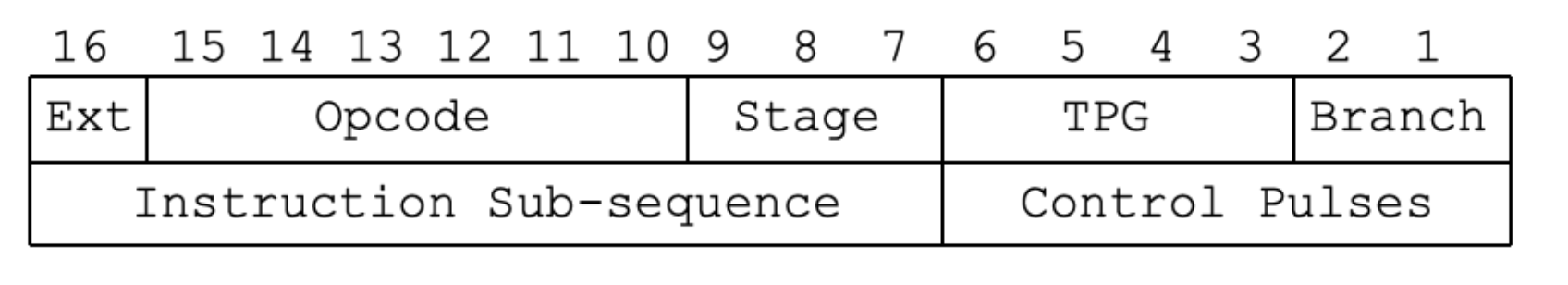
Branch state: Defines branching subsequences. bit 1 = BR2 bit 2 = BR1
Timing Pulse Generator(TPG) state: Defines the TPG stage (see TPG. module above)
Stage state: Defines the stage (instruction sub-sequence, see SEQ. module above)
Opcode: Defines the opcode of the instruction. (from the SQ register bits 10-16, see Seq. module above) This includes the quarter code and the channel bit.
Instruction Sub-sequence: Defines the instruction sub-sequence to run (see Seq. module above)
Control Pulses: Defines a specific set of control pulses for a given timing pulse.
The counter sub-sequences determine if counters need to be modified. Only the PINC sub-sequence is implemented. The PINC sub-sequence is internally generated and is not an instruction that can be externally used in the assembly code. The concept is called cycle stealing. The PINC is accessed within the control pulse matrix by setting the instruction sub-sequence to all ones.
The control pulses are defined in the Control Pulse Matrix wiki page. Table 32-5 in the AGC Information Series Issue 32, Block II Machine Instructions document defines each control pulse. Table 32-4 in the same document defines the control pulse matrix for each subsequence by timing pulse, by branch. There are 72 control pulses defined by this matrix.
The control pulse matrix is divided into three sections. Section A implements the logic described above.
Section B implements reading and writing of the registers in the lowest address locations; 0 - 27 octal. Reading and writing of the registers in address 0 - 15 use the RSC and WSC control pulses. These control pulses are translated into individual control pulses based on the address. The following is a table of these registers and their octal addresses. Note that the first seven are considered the “Central Registers” and the next seven are considered the “Special Registers.
00 = A register
01 = L register
02 = Q register
03 = EB register
04 = FB register
05 = Z register
06 = BB register
07 = all zeros
10 = ARUPT (A register)
11 = LRUPT (L register)
12 = QRUPT (Q register)
13 = spare
14 = spare
15 = ZRUPT (Z register)
16 = BBRUPT
17 = BRUPT (next instruction)
Addresses 20 - 23 are special shift and rotate locations. Writing to these addresses causes the system to shift or rotate the data right or left. This shifting is implemented in the MBF module. They are as follows:
20 = CYR (rotate right) Results: 01 15 14 13 12 11 10 09 08 07 06 05 04 03 02
21 = SR (shift right) Results: 15 15 14 13 12 11 10 09 08 07 06 05 04 03 02
22 = CYL (rotate left) Results: 14 13 12 11 10 09 08 07 06 05 04 03 02 01 15
23 = EDOP (shift 7 to right) Results: xx xx xx xx xx xx xx xx 14 13 12 11 10 09 08
The remaining addresses are contained in RAM and have special purposes.
Section C implements the control pulses to drive the memory cycle. The memory cycle occurs within one MCT and contains 12 timing pulses. This occurs no matter what instruction is being executed. The basic memory cycle is key to memory access. During a single memory cycle, data is read from memory and then new data is written to memory.
The actions per timing pulse are as follows:
TP1: Load the address into the S register.
TP4: Read from erasable memory (RAM) if address < 03777. Place data into G reg.
TP6: Read from fixed memory (ROM) if address > 03777. Place data into G reg.
TP7 - TP9: Data read is available in G register. If data needs to be written to RAM, place date into G register.
TP10: Write G register to RAM memory.
TP12: Always used to get next instruction.
The Interrupt (INT) module processing occurs when a high priority event causes the normal instruction execution to be suspended for the high priority event to be handled. This is key to a realtime system. There are two distinct types of interrupts; counter interrupts and program interrupts. Counter interrupts occur between any two instructions and consume one memory cycle. In this implementation only the PINC interrupt is implemented. The PINC sub-sequence increments a counter by one. Program interrupts also occur between any two instructions, but transfer control to an interrupt service routine. This module deals with the program interrupts. The counter interrupts are handled by the counter module.
These high priority events are handled when a RUPT signal occurs. Each RUPT signal causes the processing to save off certain registers that are later restored and depending on the RUPT signal, processing is transferred to a specific RUPT handler routine. The saved registers include the A, B, Q and L registers. If more registers need to be modified during an interrupt handling routine, the routine must handle the saving and restore of the given register. In general, interrupt routines should be as minimal as possible and should not occur too frequently. The AGC code places a job on the job list so upon return the job can be executed to process the actual event.
The normal instruction sequence can inhibit interrupts for a brief period of time if it is in a critical section of code that cannot be interrupted. Interrupt routines themselves cannot be interrupted, therefore the system needs to remember which interrupts have signaled and work off the list of interrupts until all are satisfied. The INHINT and RELINT statements inhibit and restore interrupts in normal code execution.
Four of the original eleven interrupts are implemented in this implementation. They are T3RUPT, T4RUPT, KEYRUPT1 and GOPROG. T3RUPT is an internal interrupt triggered by the counter module when the TIME3 counter overflows. T4RUPT is triggered when the TIME4 counter overflows. KEYRUPT1 is triggered when the user presses a key on the keyboard. GOPROG is triggered by various hardware that causes a hardware reset.
Address 04000, the start of fixed memory, contains a vector interrupt table consisting of 11 interrupts. The Block II computer defines the following interrupts.
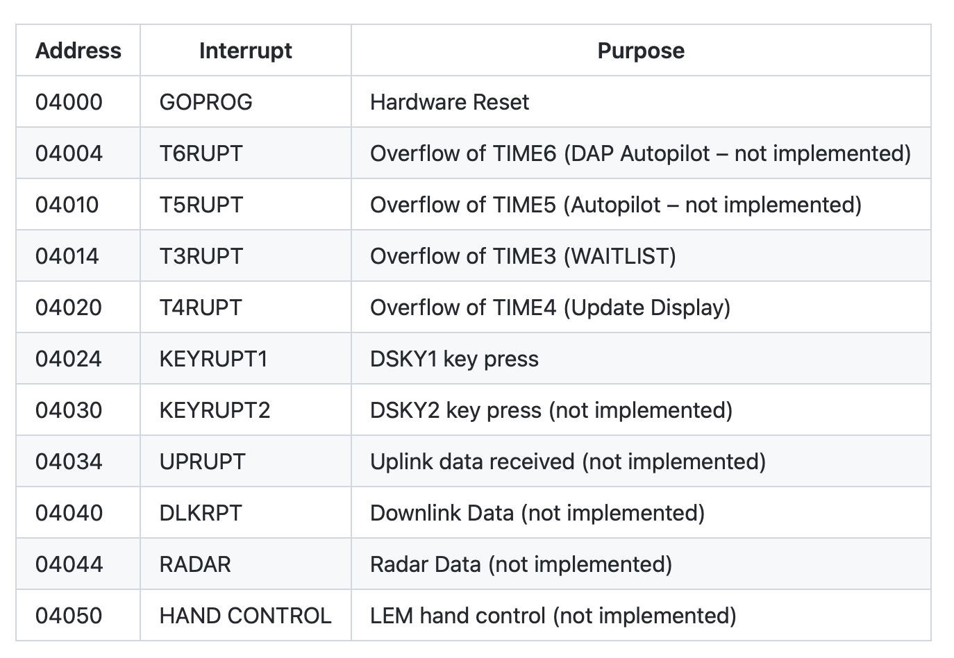
The Counters (CTR) module consists of addressable up/down counters that are controlled by various signals including Load, Read, Diminish, Shift 1, Shift 0, + increment and - increment. Priority of the counter is based on the address where address 024 is the highest priority and 060 is the lowest priority. The counters are contained in erasable memory. These subsequences occur between other instruction subsequences using “cycle stealing”.
The Block II AGC has 29 counters. Four counters are implemented in this version, the first four TIME counters. These only use the PINC sub-instruction, therefore the remaining involuntary instructions will not be implemented. The counters, their address and purpose are as follows:
| Address | Counter | Instruction |
|---|---|---|
| 024 | TIME2 | PINC |
| 025 | TIME1 | PINC |
| 026 | TIME3 | PINC |
| 027 | TIME4 | PINC |
| 030 | TIME5 | PINC |
| 031 | TIME6 | DINC |
| 032 | CUDX | PCDU, MCDU |
| 033 | CUDY | PCDU, MCDU |
| 034 | CUDZ | PCDU, MCDU |
| 035 | CDUT | PCDU, MCDU |
| 036 | CDUS | PCDU, MCDU |
| 037 | PIPAX | PINC, MINC |
| 040 | PIPAY | PINC, MINC |
| 041 | PIPAZ | PINC, MINC |
| 042 | Q-RHCCTR | PINC, MINC |
| 043 | P-RHCCTR | PINC, MINC |
| 044 | R-RHCCTR | PINC, MINC |
| 045 | INLINK | SHINC, SHANC |
| 046 | RNRAD | SHINC, SHANC |
| 047 | GYROCMD | DINC |
| 050 | CDUXCMD | DINC |
| 051 | CDUYCMD | DINC |
| 052 | CDUZCMD | DINC |
| 053 | CDUTCMD | DINC |
| 054 | CDUSCMD | DINC |
| 055 | >td >DINC | |
| 056 | EMS | DINC |
| 057 | OUTLINK | SHINC |
| 060 | ALTM | SHINC |
TIME1: The low order bits of the AGC clock. Incremented by the F10 (100 Hz) signal from the scalar. Represents 0 to 163.84 seconds. Upon overflow, it increments the TIME2 counter.
TIME2: The high order bits of the AGC clock. Incremented by the overflow of TIME1. Represents 168.84 to just over 31 days, plenty of time for an Apollo mission.
TIME3: The task timer used to manage the waitlist. When it overflows, the T3RUPT interrupt signal occurs.
TIME4: A special purpose timer used by software to update the DSKY display. When it overflows, the T4RUPT interrupt signal occurs.
TIME5 and TIME6 are not implemented along with the remainder of the counters.
The Parity (PAR) module generates and tests the memory parity bit. This bit is not enough to correct memory errors, but is enough to indicate an error occurred. The 16th bit of every word in memory is the odd parity bit. Data written to memory is made odd by the 16th bit. If a word read from memory does not have odd parity, then a parity alarm is generated. The word to be checked is written to the P register.
In Block I there were control pulses to generate and to test parity. For Block II there are no parity pulses in the Control Pulse Matrix because every time memory is written, the parity bit needs to be generated. Every time erasable memory is read, the parity bit needs to be checked.
The Memory Address (ADR) module determines the memory address based on the S register and the Bank registers. Block I had a simple 4-bit bank register for the fixed memory and no bank register for the erasable memory. Block II replaces the single bank register with a 3-bit erasable bank (EB) register, a 5-bit fixed bank (FB) register, a 16-bit both banks (BB) register that contains the same information as in the EB and FB registers and the fixed extension (FEB or Superbank) bit which resides in output channel 7.
Most if not all computers store programs on tape or disk and move the program to RAM for execution. Disk drives were not available at the time and the developers actually considered using an on-board tape drive. It was decided to “burn” the program code into fixed memory. This made the system much more durable and reliable.
The first two banks of memory are erasable memory with the remainder of the banks being fixed memory. The erasable memory address space is divided into eight erasable banks of 0400 words each. This is smaller than the fixed memory banks in that four erasable memory banks fit into one fixed memory bank. Each fixed memory bank consists of 1,024 words.
The erasable memory in Block II was doubled from 1,024 words to 2,048 words. They are accessed using the 10 least significant bits of the S register and the 3-bit EB register. The first 1,024 words can be accessed using the lower 10 bits of the S register. If bits 9 and 10 of S are both 1, then the EB register is used. The EB register can always be used if desired. This implementation needs to take both into consideration as sometimes the EB register is not set correctly.
The fixed memory words are addressed by using all 12 bits of the S register and the five bits of the FB register along with the fixed extension bit. If bit 12 is set to 1 then bits 1-11 are used to define first block of 2048 words of fixed memory. If bits 12-11 are set to 01 then the FB register is used to address the next 37 blocks of 1027 words. The FEB bit is used to to address the next blocks of memory.
The bank's CPU address, the address used by the code, overlap and when they overlap, the bank address must be used. There are a few banks that can be directly addressed using the full 12 bit address. The hardware address is the address used to access the code in the EPROM. To determine the hardware address, you start with the CPU address.
A CPU address of 0000-0377 represents the first bank of erasable memory named E0. The first three erasable memory banks represent un-switched erasable memory. The remaining five erasable memory banks are called switched erasable memory. These switched erasable banks all have a CPU address of 1400-1777 and must use the erasable bank value.
A CPU address of 02000-03777 represent common fixed memory addresses. All fixed memory banks have this CPU address range except the two fixed-fixed memory banks. These map to F2 and F3 fixed memory banks. F2 has a CPU address range of 04000-05777 and F3 has a CPU address range of 06000-07777. Notice that the F0 and F1 banks overlap the addresses of erasable memory. This is OK because they are only used to access the EPROMs.
The following table maps out the memory.
| CPU Addr. Range | H/W Addr. Range | Designation |
|---|---|---|
| Erasable Memory: | ||
| 00000–00377 | 00000-00377 | E0 |
| 00400–00777 | 00400-00777 | E1 |
| 01000–01377 | 01000-01377 | E2 |
| 01400-01777 | 01400-01777 | E3 |
| 01400-01777 | 02000-02377 | E4 |
| 01400-01777 | 02400-02777 | E5 |
| 01400-01777 | 03000-03377 | E6 |
| 01400-01777 | 03400–03777 | E7 |
| Fixed Memory: | ||
| 04000-05777 | 04000-05777 | F2 |
| 06000-07777 | 06000-07777 | F3 |
| 02000-03777 | 10000-11777 | F4 |
| 02000-03777 | 12000-13777 | F5 |
| 02000-03777 | 14000-15777 | F6 |
| . . . | ||
| 02000-03777 | 66000-67777 | F33 |
| 02000-03777 | 70000-71777 | F34 |
| . . . | ||
| 02000-03777 | 106000-107777 | F43 |
The EB register consists of 3 bits. The FB register consists of 5 bits. The FEB register consists of one bit. When the bank number is written into either the EB or FB registers, the values are available in the Both Banks (BB) register such that the BB register contains FFF FF0 000 000 EEE. Bit 7 of Channel 07 contains the FEB bit.
The erasable memory banks E3 - E7 are identified because bits 12-9 of the address are always “0011”. The EB register is then used to determine the bank. The first bank of fixed memory is defined by bit 12 being set. The remainder of the fixed banks are defined by bits 12-11 having a value of “01”. The FB register defines the next 32 banks. Additional banks are defined by setting the fixed extension bit. These are the superbanks.
The Memory Buffer (MBF) module contains the G register. All data written into and read out of memory must go through the G register. The data can be shifted or rotated left or right by writing it to memory locations 020 - 023. This is accomplished by the W20 - W23 control pulses.
The WE control pulse writes to memory. In memory the 16th bit is the parity bit and the 15th bit is the sign bit. The SBWG control pulse reads data from memory and places it into the G register. Data is moved from the write bus into the G register with the WG control pulse. The other four control pulses shift/rotate the bits right or left. The RG control pulse reads data from the G register onto the read bus. The parity bit is replaced with a copy of the sign bit.
The resulting bit pattern is not obvious so there is a bit map showing the results after the shift/rotate. Data bits are represented by B1-B14. SG is the sign bit and BX is a don't care.
WE: BX,SG,B14,B13,B12,B11,B10,B9,B8,B7,B6,B5,B4,B3,B2,B1
SBWG: SG,BX,B14,B13,B12,B11,B10,B9,B8,B7,B6,B5,B4,B3,B2,B1
RG: SG,SG,B14,B13,B12,B11,B10,B9,B8,B7,B6,B5,B4,B3,B2,B1
W20: rotate right one bit: B1,BX,SG,B14,B13,B12,B11,B10,B9,B8,B7,B6,B5,B4,B3,B2
W21: shift right one bit: SG,BX,SG,B14,B13,B12,B11,B10,B9,B8,B7,B6,B5,B4,B3,B2
W22: rotate left one bit: B14,BX,B13,B12,B11,B10,B9,B8,B7,B6,B5,B4,B3,B2,B1,SG
W23: shift right seven bit: BX,BX,BX,BX,BX,BX,BX,BX,BX,B14,B13,B12,B11,B10,B9,B8
The Erasable/Fixed Memory (EFM) module contains the fixed memory and the erasable memory. The erasable memory is divided into banks of 256 16-bit words. The fixed memory is divided into banks of 1024 16-bit words. The fixed memory banks contain the program and they will be placed into an EPROM. The original memory was core memory. The little doughnuts of magnetic material had to be “sewn” together. This was a two person job requiring the help of a computer to get the sequence of 1s and 0s correct.
The Display (DSP) module is part of the DSKY that includes the 7-segment displays along with the indicator lamps. The indicators include computer activity, uplink activity, temperature, no attitude, gimbal lock, standby, program alarm, key release, restart, operator error, tracker, altitude and velocity. The 7-segment displays include three 2-digit numbers for the program, verb and noun. There are three 5-digit general purpose numbers named R1, R2 and R3. These had a leading +/- sign. Since a 7-segment LED can produce a minus but not a plus and the sign indicated the number being displayed is decimal versus octal, a new indication is required. For decimal numbers, a leading minus sign will be utilized, however for a positive number, a far left decimal point will be shown. This means each of the three “register” displays will consist of six 7-segment displays. The display therefore consists of 24 7-segment displays. The Noun and Verb digits flash to indicate the operator needs to perform some action.
The indicator lamps are lit for the following reasons.
COMP ACTY : The computer is busy.
UPLINK ACTY : Data is being received from ground control.
TEMP : The IMU temperature is out of tolerance.
NO ATT : The inertial subsystem could not provide an attitude reference.
GIMBAL LOCK : The middle gimbal angle is greater than 70 degrees.
STBY : The computer is in standby.
PROG : The computer is waiting for operator input.
KEY REL : The computer wants to display data but the astronaut is inputting data.
RESTART : The computer is restarting.
OPR ERR : There was a data entry error.
TRACKER : One of the optical coupling units failed.
ALT : The altitude is out of range.
VEL : The velocity is out of range.
The RESTART light is not directly connected to a channel, but is lit based on a number of possibilities. Per R-700, figure 3-14 there are seven possible reasons to light this light. I have implemented two of the possibilities; a parity failure and going to standby mode. Here are a list of the possibilities. All of these would cause a restart.
Parity Fail – Memory parity upon read is not odd.
Night Watchman – Computer software fails to access address 067 at least every 0.64 seconds.
RUPT Lock – If interrupt has not occurred in the last 140 milliseconds or lasts longer than 140 milliseconds.
TC Trap – If a TC or TCF instruction has not occurred in the last 5 milliseconds or continuously for 5 msecs.
OSC Failure – The oscillator stops running.
Voltage Failure – The 4, 14 or 28 volt power supplies go outside the limits.
Standby – The computer is commanded to go to standby.
The Keyboard (KBD) module implements the user keyboard of the DSKY. There are 19 keys; the 10 numeric keys, a plus and minus key, a verb and noun key, an enter/execute key, an error reset key, a key release key, a proceed key and a clear key. The proceed key was added for Block II. The key codes are defined in the Channel module.
It is interesting to note that user interfaces were in their infancy at this time. The DSKY interface feels like a calculator. Most of the astronauts did not like the interface. As test pilots, they wanted gauges and dials like an airplane.
The LEM had one DKSY and the Command Module had two; one that was accessible from the chairs and one below to input navigation measurements. For this reason I am targeting the LEM software since it only supported one DSKY.
The keyboard and display are described in the document E-1574 - “Keyboard and Display System Program for AGC (Program Sunrise)”. Of particular interest are the flow diagrams at the end of the document describing the actual code. The keyboard keys and their use are as follows.
STBY : Places the computer in standby.
RESET : Turns off the indicator lamps.
KEY REL : Releases DSKY to computer control so the program can display data.
CLR : Clears the current display.
VERB/NOUN/ENTER : Enter a command.
0-9/+/- : Self explanatory.
The channel implementation is implemented in various modules, but discussed here as one consistent concept. The registers are contained within the module most closely related to their functionality. For example, channel 10 which is used to output data to the display is contained within the Display module. The common portions of the channel implementation are contained within the Central Registers module because many of the commands combine the channel data with the A register.
In the Block I design, the input and output registers were located in the erasable memory address space. This is a method known as memory mapped I/O. In Block II the channels were moved to their own address space. The L and Q registers have addresses in both address spaces. This is so that they are able to take advantage of the OR and XOR I/O instructions. The channels have the following octal addresses. Note that these definitions, especially the bit definitions, are defined for Luminary 099 and Comanche 055. The bit definitions can be expected to change from version to version.
| Address | # bits | Purpose |
|---|---|---|
| 1 | 16 | |
| 16 | ||
| 14 | High order time scaler (not implemented) | |
| 4 | 14 | Low order time scaler (not implemented) |
| 5 | 8 | OUTPUT: PYJets: pitch and yaw RCS jets (not implemented) |
| 6 | 8 | OUTPUT: RollJets: roll RCS jets (not implemented) |
| 7 | 3 | Fixed memory extension bits |
| 10 | 15 | OUTPUT: OUT0: DSKY display command |
| 11 | 15 | OUTPUT: DSALMOUT: DSKY status lights |
| 12 | 15 | OUTPUT: GN&C/LM radar control & LM gimbal (not implemented) |
| 13 | 15 | OUTPUT: LM radar select, I/F mode control (not implemented) |
| 14 | 15 | OUTPUT: counters, LM thrust & alt. meter (not implemented) |
| 15 | 5 | INPUT: Main DSKY keyboard |
| 16 | 7 | INPUT: CM Nav DSKY keyboard(not implemented) |
| 30 | 15 | INPUT: GN&C and Spacecraft mode (not implemented) |
| 31 | 15 | INPUT: Hand controllers & Spacecraft mode (not implemented) |
| 32 | 15 | INPUT: Contains PRO key press and other unimplemented bits |
| 33 | 15 | INPUT: CM optics, LM radar & failure mode (not implemented) |
| 34 | 16 | OUTPUT: downlink first word (not implemented) |
| 35 | 16 | OUTPUT: downlink second word (not implemented) |
| 77 | 9 | INPUT: restart monitor bits (not implemented) |
Only seven of the channels are implemented; two DSKY output channels (10 & 11), two DSKY input channels (15 & 32), the extension bit channel (7) and the L & Q registers (1 & 2). Within this document, only the channels and bits that are implemented are described. The channel bus is 15-bits in length.
The input channels 15 and 16 contain five bits that can handle up to 32 key press values. Channel 15 is the Main DSKY and channel 16 is the Navigation DSKY. Channel 16 for the LM has bits used for other purposes. The following table lists the key codes, in octal, for key presses along with the purpose for some keys.
| Key Name | Value | Purpose |
|---|---|---|
| No key | 00 | |
| 1 | 01 | |
| 2 | 02 | |
| 3 | 03 | |
| 4 | 04 | |
| 5 | 05 | |
| 6 | 06 | |
| 7 | 07 | |
| 8 | 10 | |
| 9 | 11 | |
| 0 | 20 | |
| Verb | 21 | Used to enter a verb value. |
| Reset | 22 | Acknowledge and turn off error lights. |
| Key Rel | 31 | If Key Release light is on, computer wants control of DSKY to display important data. Press this key to give up control. |
| "+" | 32 | |
| "-" | 33 | |
| Enter | 34 | Accept entered or supplied Noun/Verb command. |
| Clear | 36 | Clear command entered so far if error is made. |
| Noun | 37 | Used to enter a noun value. |
| PRO(STBY) | Go into/out of standby mode. |
Input channel 32, bit 14 indicates the PRO(STBY) key is pressed. The logic is inverted. 0 indicates the key is pressed, 1 indicates the key is released. The other bits are not implemented as they relate to engine control.
Output channel 11 is named DSALMOUT and drives the indicator lamps using the following bits.
| Bit | Purpose |
|---|---|
| 1 | Not implemented |
| 2 | Computer Activity Lamp |
| 3 | Uplink Activity Lamp |
| 4 | Temp Caution Lamp |
| 5 | Key Release Lamp |
| 6 | Flash Verb/Noun Lamps |
| 7 | Operator Error Lamp |
| 8- 15 | Not implemented |
Output channel 13 drives an indicator lamp and performs light and alarm test using the following bits.
| Bit | Purpose |
|---|---|
| 1-9 | Not implemented |
| 10 | Test alarms and DSKY lights |
| 11 | Enable Standby |
| 12-15 | Not implemented |
Output channel 10 is used to drive the 7-segment displays as pairs of numbers. Each output of the OUT0 register can drive two 7-segment numbers. The format of the register is bits 1-5 hold the right hand digit value (DSPL), bits 6-10 hold the left hand digit value (DSPH), bit 11 indicates the verb and noun digits should be flashing (DSPC) and bits 12-15 contain the relay word (RLYWD).
RRRRFHHHHHLLLLL
The relay word tells the system which two digits this is describing. The following table shows the relay word values and which two digits to update. For R1-R3 the digits are labeled RxS for sign digit followed by RxD1, RxD2, RxD3, RxD4 and RxD5.
| RLYWD | # | DSPC | DSPH | DSPL |
|---|---|---|---|---|
| 1011 | 11 | n/a | Prog1 | Prog2 |
| 1010 | 10 | Flash | Verb1 | Verb2 |
| 1001 | 9 | n/a | Noun1 | Noun2 |
| 1000 | 8 | UPACT | n/a | R1D1 |
| 0111 | 7 | +R1S | R1D2 | R1D3 |
| 0110 | 6 | -R1S | R1D4 | R1D5 |
| 0101 | 5 | +R2S | R2D1 | R2D2 |
| 0100 | 4 | -R2S | R2D3 | R2D4 |
| 0011 | 3 | n/a | R2D5 | R3D1 |
| 0010 | 2 | +R3S | R3D2 | R3D3 |
| 0001 | 1 | -R3S | R3D4 | R3D5 |
| 0000 | 0 | (inactive state) | ||
| 1100 | 12 | Lights various lights (see below) |
Relay word 12:
Bit 1 - PRIO DISP indicator (not used)
Bit 2 – NO DAP indicator (not used)
Bit 3 – VEL indicator
Bit 4 – NO ATT indicator
Bit 5 – ALT indicator
Bit 6 – GIMBAL LOCK indicator
Bit 8 – TRACKER indicator
Bit 9 – PROG indicator
The following table lists the values fr the two 5-bit digit values. The values stored in memory are 1's compliment values.
| Digit | MSB – LSB | 1's comp |
|---|---|---|
| Blank | 00000 | 11111 |
| 0 | 10101 | 01010 |
| 1 | 00011 | 11100 |
| 2 | 11001 | 00110 |
| 3 | 11011 | 00100 |
| 4 | 01111 | 10000 |
| 5 | 11110 | 00001 |
| 6 | 11100 | 00011 |
| 7 | 10011 | 01100 |
| 8 | 11101 | 00010 |
| 9 | 11111 | 00000 |
The remaining channels are not implemented in this implementation.
The Monitor (MON) module is added for debugging purposes. This corresponds to the AGC simulator GUI interface. This module contains lots of LEDs that are connected to various registers and buses. There are also many switches that allow you to debug the system by single stepping through instructions and sub-sequences as well as stepping the clock. This functionality is not part of the original system and almost doubles the chip count, but makes debugging hardware much easier and who doesn’t like computers with flashing lights?
The switches are heavily based on John's design. I added the ability to set breakpoints on interrupts, counter overflow and specific addresses. I also modified and upgraded the LEDs and switches from Block I to a Block II configuration.
Discussions
Become a Hackaday.io Member
Create an account to leave a comment. Already have an account? Log In.