Up to this point I have been in my comfort zone, having spent my career as a software developer. Now it is off into the unknown of hardware development. The first thing I need is a good schematic drawing tool. After some research I decided to use KiCad. It is free, easy to use and seems to be what all the cool kids are using.
Note that all my schematics are out on my GitHub site at https://github.com/bglasford1 under the AGC Block II Computer project in the schematics directory. I chose to divide the project into five sub-systems; DSKY, Control, Processor, Memory and Display. The DSKY sub-system consists of the Keyboard, Display and Indicator modules. The Control sub-system contains the Clock, Scalar, Timing Pulse Generator, Sequence, and Control Pulse Matrix modules. The Processing sub-system contains the Arithmetic Logic Unit and Central Register modules. The Memory sub-system contains the Erasable Fixed Memory, Memory Buffer, Parity, Memory Address, Interrupts and Counters modules. The Display sub-system contains the Monitor module along with all the LEDs and switches from the Control, Processing and Memory sub-systems. The basis for splitting the modules up into sub-systems was to group like modules and to evenly divide them onto individual boards based on initial chip count.
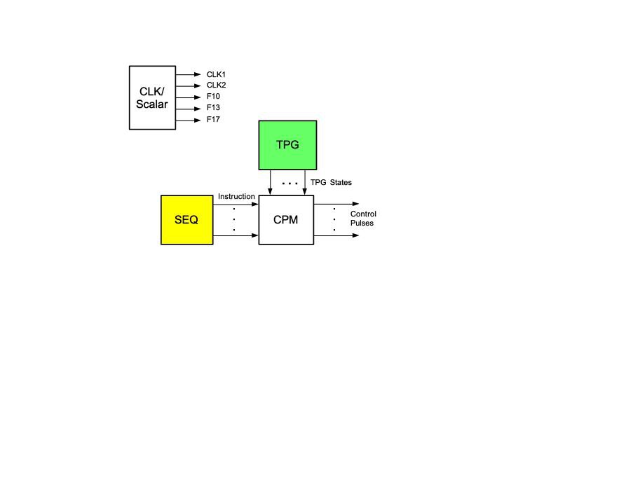
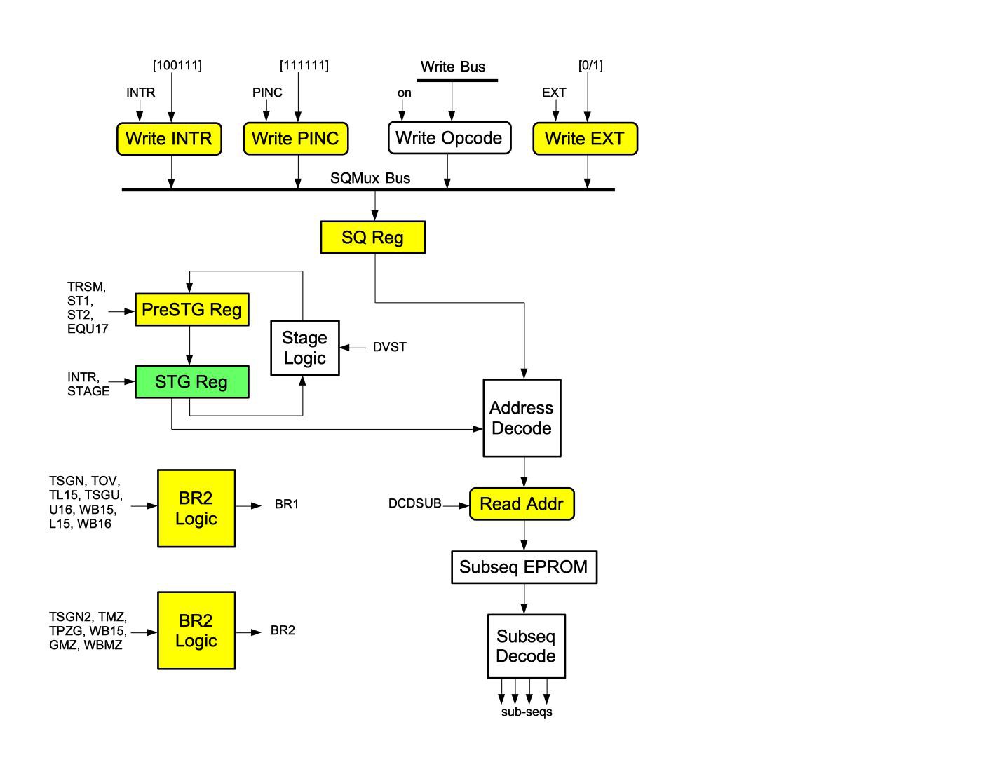
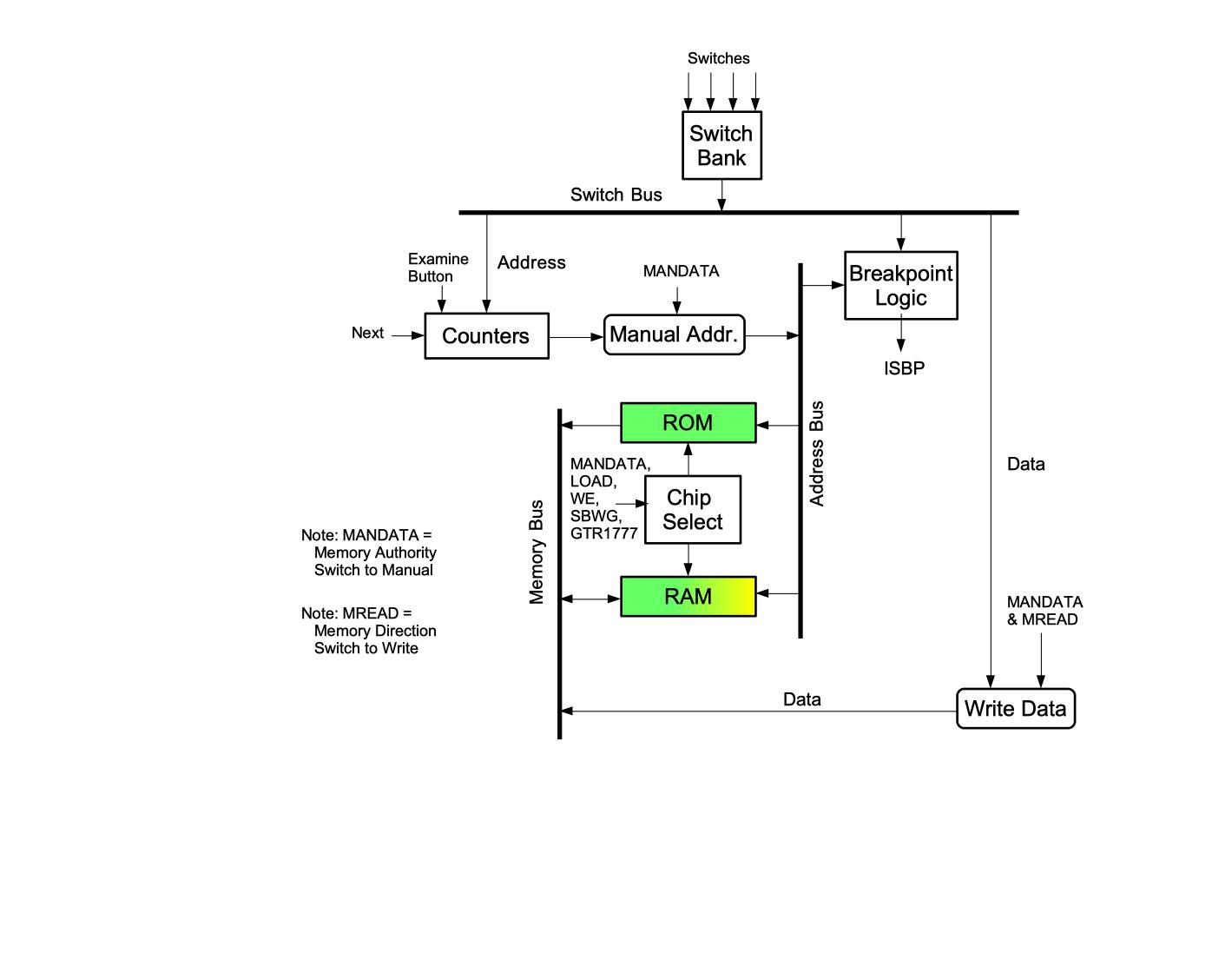
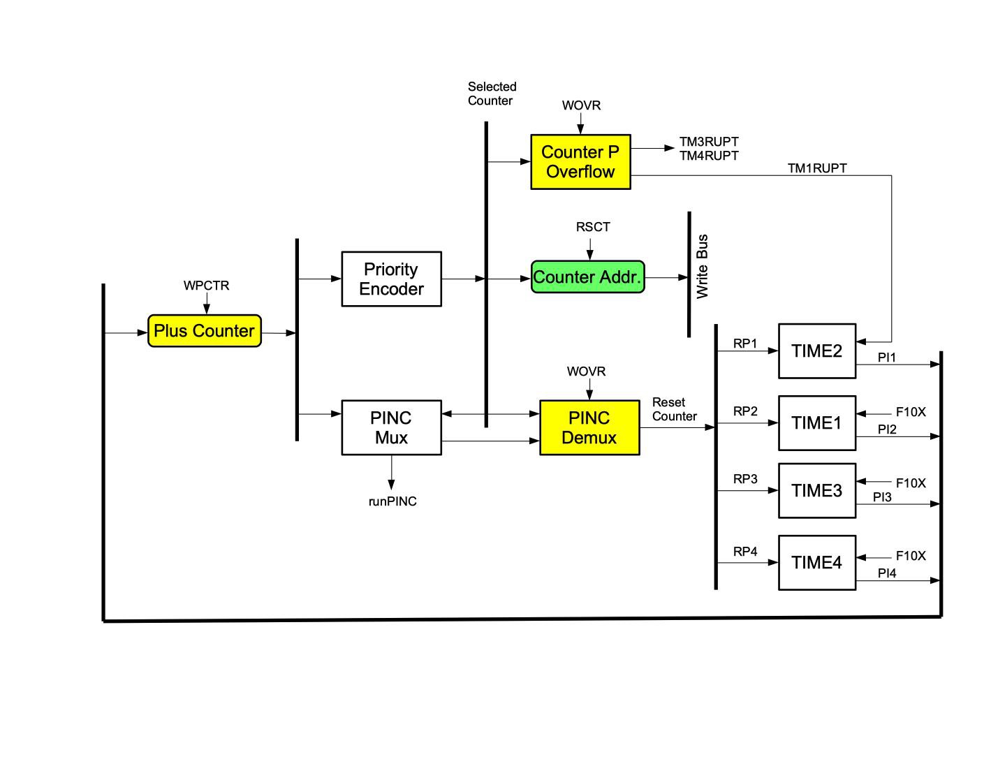
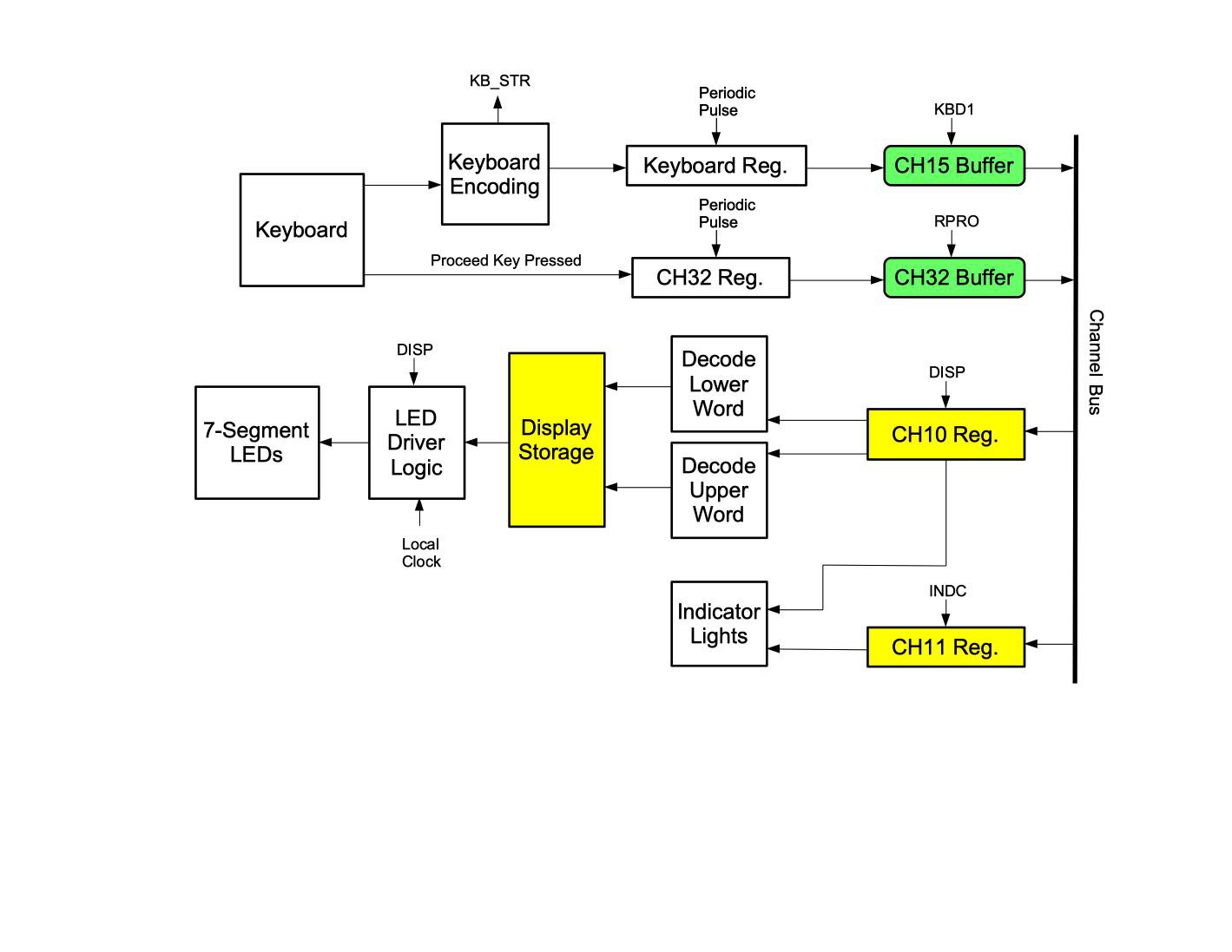
I first had to create some data flow diagrams to visualize how this beast would be wired together and what pieces relate to other pieces. The data flow diagrams depict how the buses and registers interact with the control signals. The registers and logic blocks are rectangles and the bus drivers are round-tangles. The control signals that drive data into/out of registers and bus drivers are shown. The bus drivers and registers that are activated by the CLK1 pulse are colored green, the ones activated by the CLK2 pulse are colored yellow and the ones activated by the CLK3 pulse are colored cyan. This allows a quick visualization of the multi-stage data flow control during a single timing pulse.
The following data flow diagram shows the overview of the control sub-system which includes the Timing Pulse Generation, Sub-sequence and Control Pulse Matrix modules as well as the Clock and Scalar modules. The Clock and Scalar modules simply create various clock pulses. The Timing Pulse Generation module uses a slightly delayed CLK1 pulse to transition between 12 timing pulse states as well as a few other debug states. The Sub-sequence module maintains the parts that make up the next instruction, to include the stage, sequence and branch values. These along with the timing pulse state are fed into the Control Pulse Matrix module which uses these values to look up the control signals from the control pulse matrix EPROMs. These control signals along with other internally generated signals cause the other modules to perform actions. These control pulses are generated during the rising edge of the CLK1 pulse. The other modules act on the read control signals immediately and delay the write signals until the start of the CLK2 pulse.
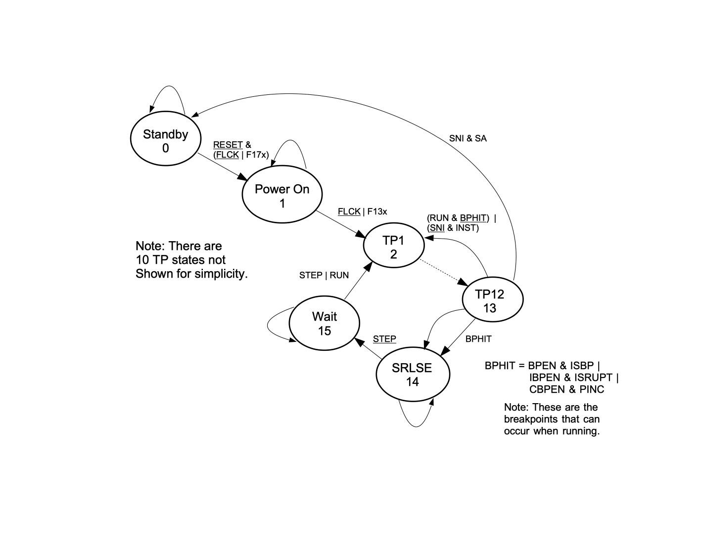
The Timing Pulse Generator is a state machine that controls the states a sub-sequence goes through. This includes the start up states and states that allow one to debug the system. Many of the states loop back on themselves, waiting for a specific input to transition them to the next state. Once in the TP1 state, the state machine transitions through to TP12 each clock pulse. The intermediate states are not shown for clarity. At TP12 the state can transition to a wait state if a breakpoint is set or to standby if the standby switch is set or loop back to TP1 if free running. Notice that if none of these states is set it simply transitions to the wait state. The wait state is preceded by the Switch Release state. Under each state name is a number that is the internal numeric depiction of the state.
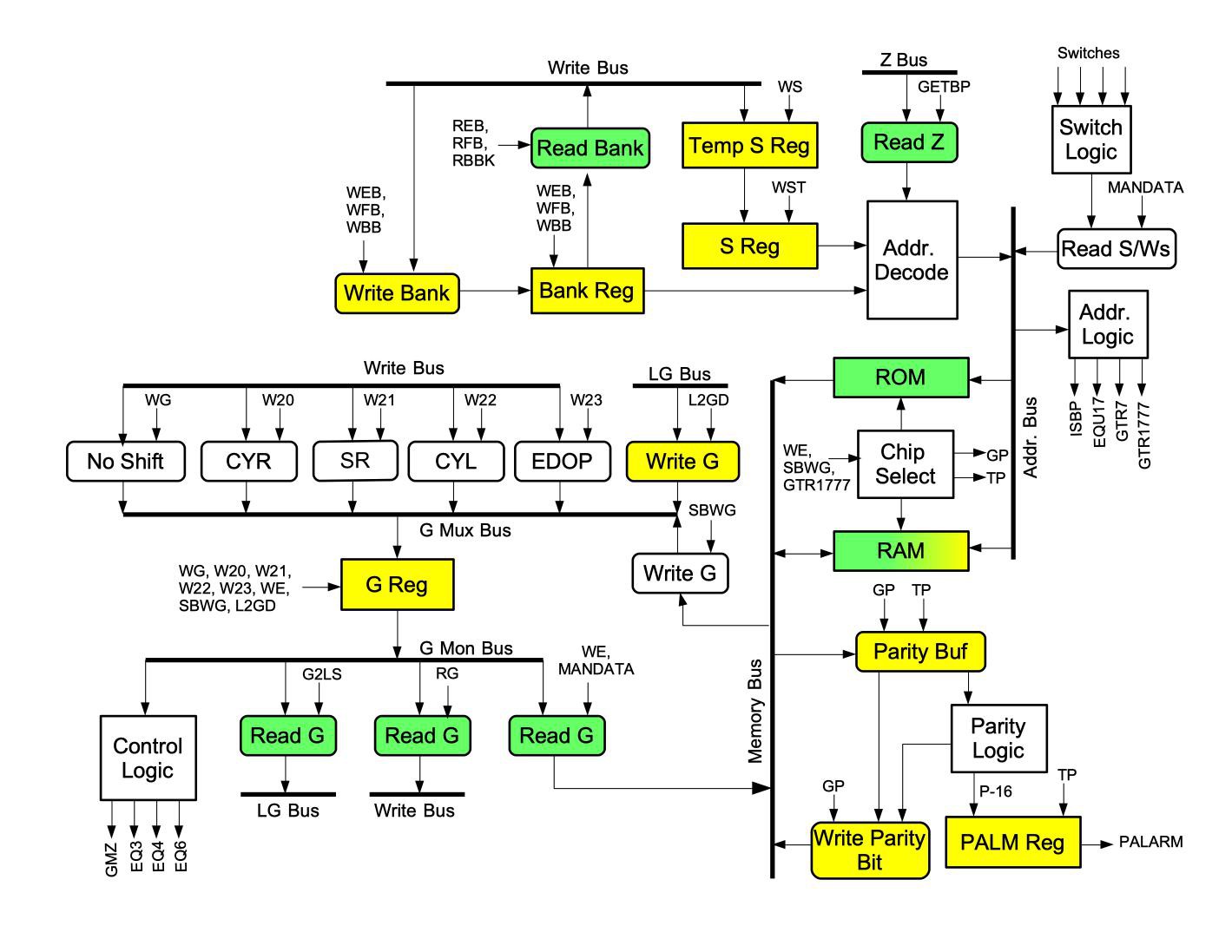
The following data flow diagram shows the memory logic and how various memory modules interact and how they are controlled by control pulses. The data written to certain values (020, 021, 022 & 023) go through shift registers before being written to the G register. All data moving onto and out of memory goes through the G register.
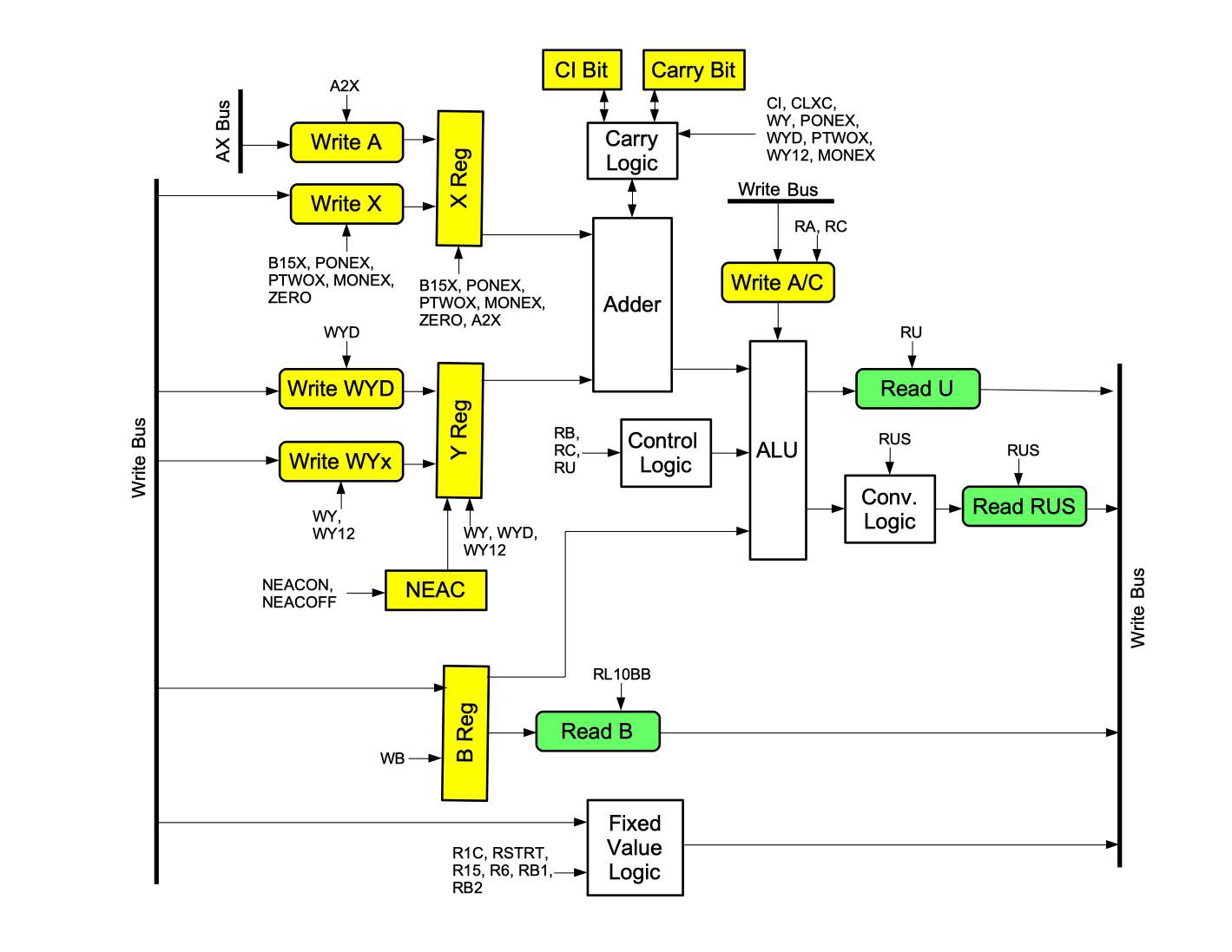
The following data flow diagram shows how the various modules that make up the Arithmetic Logic Unit interact and how the control pulses manage the logic. The X and Y registers are used as inputs to the adder that adds the two values. The results of the adder and the B register can be manipulated in various ways using a set of ALU chips. The output is considered the U register.
The following data flow diagram shows how the pieces of the Sub-sequence module interact and how the control pulses manage the logic. The Sequence register is the opcode of the next instruction unless a PINC sub-sequence or an interrupt occur. This value along with the Stage register are used to determine the next instruction sub-sequence to run. The branch values are used by the Control Pulse Matrix module to determine the next control signals to assert.
The following data flow diagram shows how the manual switches are used to read data from a given memory location, write data directly the memory bus and to check to see if a breakpoint address has been reached.
The following data flow diagram shows the counter logic. When appropriate, a runPINC control pulse is generated. This signal causes the PINC sub-sequence to run which increments the actual counter. Counters 1, 3 & 4 are incremented every 10 milliseconds when the F10X control pulse is asserted. Counter 2 is incremented when counter 1 overflows. The counter address is generated when the RSCT control pulse is asserted. This address is the address of the counter to increment.
The following data flow diagram shows the interrupt logic. There are three interrupts that can occur; RUPT3, RUPT4 and RUPT5 (keyboard data). The waiting interrupts are saved in the RPCell. When a RRPA control pulse is asserted, the current interrupt address is generated. This is the address of the jump table within the code. Interrupts can be inhibited.

The following data flow diagram shows how the DSKY is used to read data from the keyboard and write data to the 7-segment LEDs and the indicator lights.
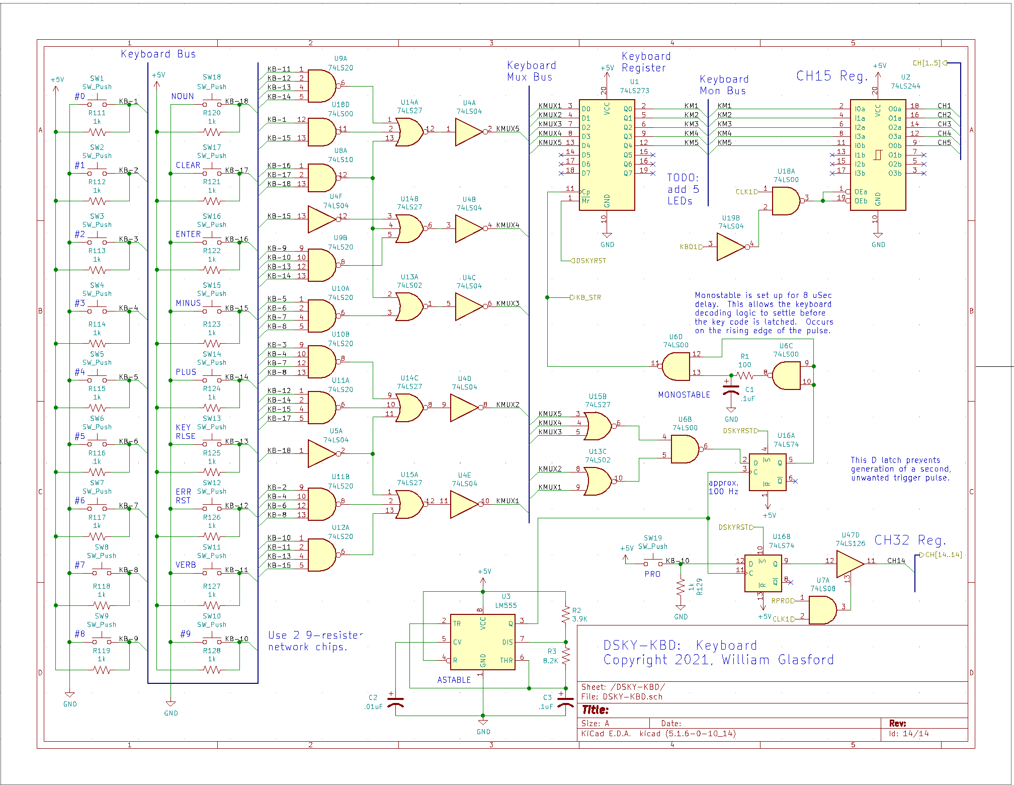
I won't show pictures of each of the pages of schematics. There are over 100 pages. If you are interested, load up KiCad and give it a try. Currently the DSKY, DISP and MEM sub-systems are out there. I have sketched out the CTL and PROC sub-systems but have not yet published them. Here is one schematic page, the Keyboard.
Discussions
Become a Hackaday.io Member
Create an account to leave a comment. Already have an account? Log In.