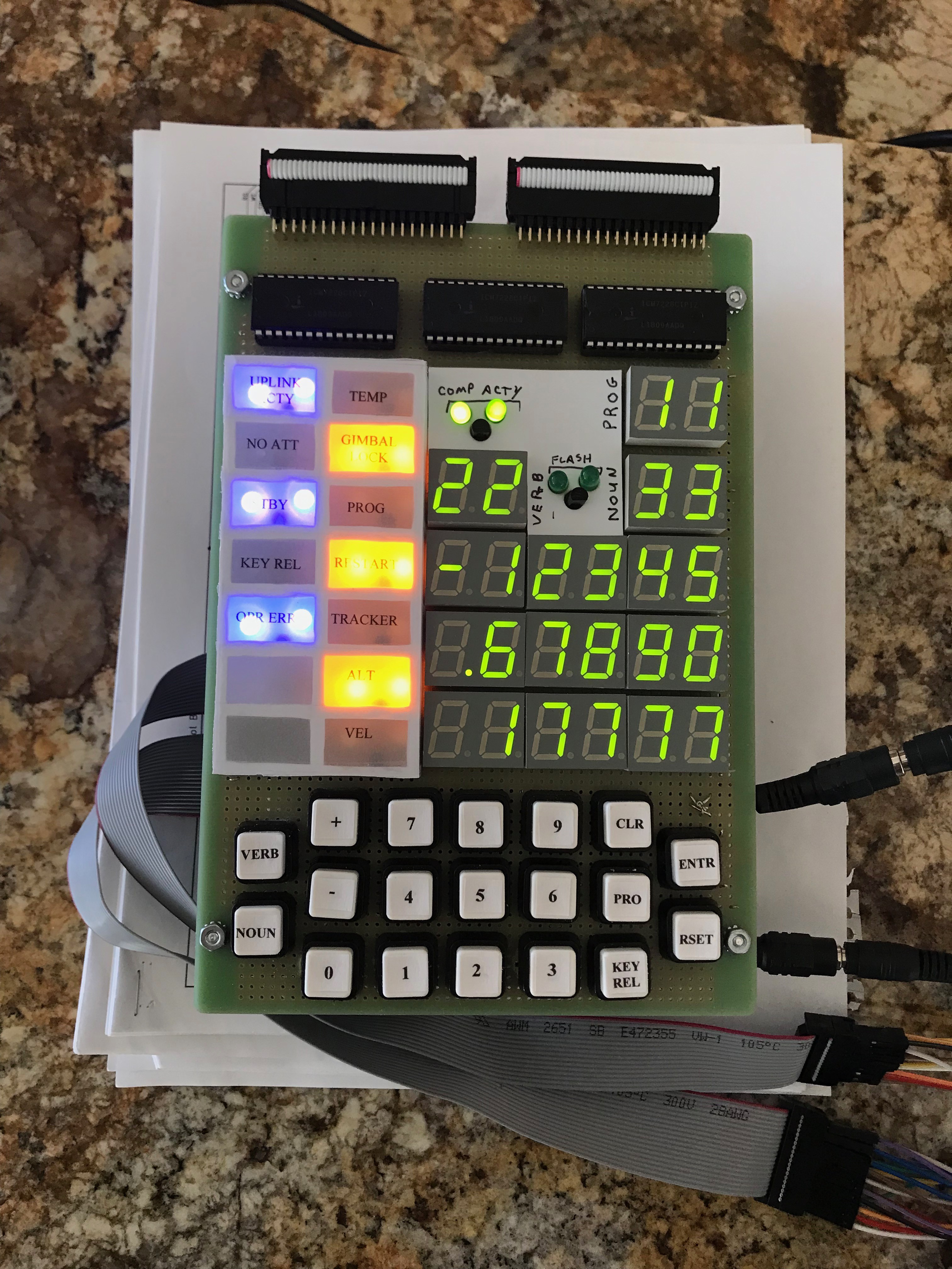
The DSKY is a separate physical piece of hardware with a simple interface consisting of the 15-bit channel bus and a handful of control signals. I built this as a stand-alone piece that started out as two boards and then grew to three boards. I have tried two different implementations and have finally settled on a third implementation. This has been slow going as during the pandemic I have been stymied with a shortage of certain chips. I first tried using only simple TTL chips and it got a bit too complex. I then discovered an LED driver chip and decided to go with those. I purchased three of these chips and discovered I needed a fourth and I have been waiting for 6 months for availability to complete this sub-system.
I test this sub-system with a Raspberry Pi driving the data lines. Here is picture of that setup.
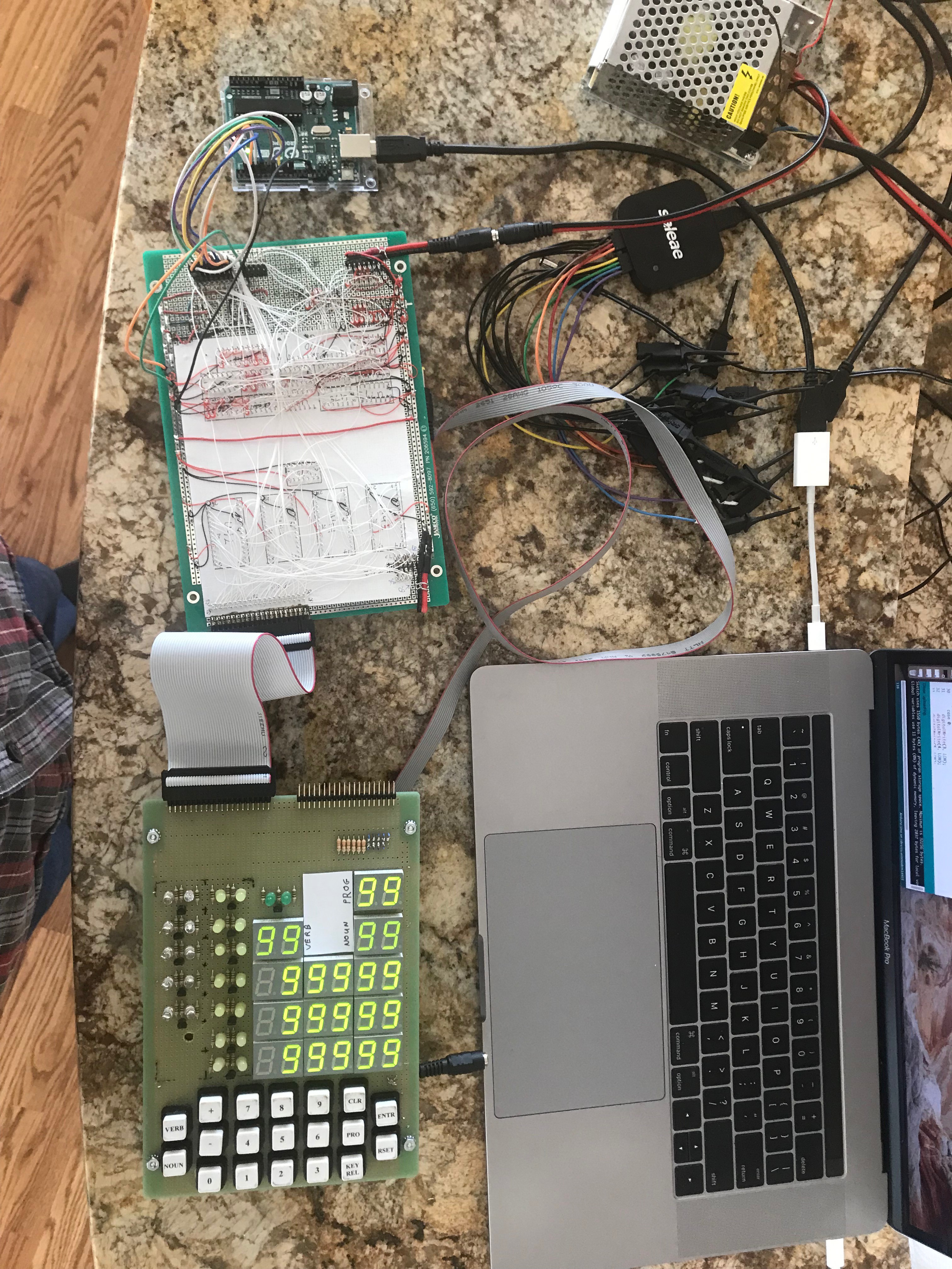
As soon as I get the remaining chips I need I will complete this sub-system. In the mean time I made a paper model of the DSKY and that sent me down the path of building a better looking model of the DSKY. See my DSKY Model project for the progress on that DSKY. Both DSKYs are designed to connect to the AGC.
Here are some of the design notes that will help understand the schematics.
Keyboard: This module implements 19 switches. These switches are converted into a keyboard code using gate logic that is stored in the Channel 15 register. The keyboard codes, their meaning are defined in the following table.
| Key | A | B | C | D | E | ID |
|---|---|---|---|---|---|---|
| 1 | 0 | 0 | 0 | 0 | 1 | 1 |
| 2 | 0 | 0 | 0 | 1 | 0 | 2 |
| 3 | 0 | 0 | 0 | 1 | 1 | 3 |
| 4 | 0 | 0 | 1 | 0 | 0 | 4 |
| 5 | 0 | 0 | 1 | 0 | 1 | 5 |
| 6 | 0 | 0 | 1 | 1 | 0 | 6 |
| 7 | 0 | 0 | 1 | 1 | 1 | 7 |
| 8 | 0 | 1 | 0 | 0 | 0 | 8 |
| 9 | 0 | 1 | 0 | 0 | 1 | 9 |
| 0 | 1 | 0 | 0 | 0 | 0 | 0 |
| Verb | 1 | 0 | 0 | 0 | 1 | a |
| Reset | 1 | 0 | 0 | 1 | 0 | b |
| Key Rel | 1 | 1 | 0 | 0 | 1 | c |
| "+" | 1 | 1 | 0 | 1 | 0 | d |
| "-" | 1 | 1 | 0 | 1 | 1 | e |
| Enter | 1 | 1 | 1 | 0 | 0 | f |
| Clear | 1 | 1 | 1 | 1 | 0 | g |
| Noun | 1 | 1 | 1 | 1 | 1 | h |
The keys are pushbuttons that are normally high. A keypress presents a zero to the logic equations. Negative logic presents the easiest solution. All the lines of interest are normally 1. The logic for each of the five code bits is looking for a key to go low. The logic equations utilize 3 and 4 input NAND gates along with 2 and 3 input NOR gates. The results is NOTed. The equations are as follows.
A = (a * b * c * d) + (e * 0) + (f * g * h)
B = (8 * 9 * c * d) + e + (f * g * h)
C = (4 * 5 * 6 * 7) + (f * g * h)
D = (2 * 3 * 6 * 7) + (b * d * e * g) + h
E = (1 * 3 * 5 * 7) + (9 * a * c * e) + h
Notice that some of the portions of the equations are the same. For instance, A, B and C both have the (f * g * h) portion.
Display: The Display module implements the Channel 10 and 11 registers. Channel 10 is used to write data to the 7-segment LEDs two LEDs at a time. Channel 11 is used to light various indicators. Eight indicator are controlled using Channel 11. Another eight are controlled using Channel 10 with a specific relay word.
It should be noted that all the miscellaneous timing pulses using 555 chips are set up as astable multi-vibrators.
Most of the display logic decodes the Channel 10 value which is used to drive the 7-segment displays as pairs of numbers. Each output to this register drives two 7-segment numbers along with the plus/minus signs and a few other indicators. The format of the register is bits 1-5 hold a low digit value (DSPL), bits 6-10 hold a high digit value (DSPH), bit 11 indicates the plus/minus sign (DSPC) and bits 12-15 contain the relay word (RLYWD).
RRRRSHHHHHLLLLL
According to Ron's website, it is unclear how to blank the sign LEDs. There is one that says light the “+” sign and one that says light the “-” sign. Ron chose to display a blank if both values are zero. There is also the case where both may be set. I am not sure if this is avoided in code, but I have decided to handle this as a blank the sign case. The following table shows the possible states and the results.
| (+) State | (-) State | Plus | Minus |
|---|---|---|---|
| 0 | 0 | 0 | 0 |
| 0 | 1 | 0 | 1 |
| 1 | 0 | 1 | 0 |
| 1 | 1 | 0 | 0 |
The relay words and the digits each one drives is listed below.
| RLYWD | # | DSPC | DSPH | DSPL |
|---|---|---|---|---|
| 1011 | 11 | n/a | MD1 | MD2 |
| 1010 | 10 | Flash | VD1 | VD2 |
| 1001 | 9 | n/a | ND1 | ND2 |
| 1000 | 8 | UPACT | n/a | R1D1 |
| 0111 | 7 | +R1S | R1D2 | R1D3 |
| 0110 | 6 | -R1S | R1D4 | R1D5 |
| 0101 | 5 | +R2S | R2D1 | R2D2 |
| 0100 | 4 | -R2S | R2D3 | R2D4 |
| 0011 | 3 | n/a | R2D5 | R3D1 |
| 0010 | 2 | +R3S | R3D2 | R3D3 |
| 0001 | 1 | -R3S | R3D4 | R3D5 |
| 0000 | 0 | (inactive state) | ||
| 1100 | 12 | Lights various | indicator lights |
The 7-segment LEDs and their names are laid out as follows on the DSKY.
| . | . | . | . | . | . |
|---|---|---|---|---|---|
| MD1 | MD2 | ||||
| VD1 | VD2 | ND1 | ND2 | ||
| R1S | R1D1 | R1D2 | R1D3 | R1D4 | R1D5 |
| R2S | R2D1 | R2D2 | R2D3 | R2D4 | R2D5 |
| R3S | R3D1 | R3D2 | R3D3 | R3D4 | R3D5 |
A decoder is required to convert from the 5-bit AGC code to a 4-bit hexadecimal number (BCD) that is understood by the BCD to 7-segment decode chips. The following table shows the two formats side-by-side.
| Num | AGC | Hex |
|---|---|---|
| 0 | 10101 | 0000 |
| 1 | 00011 | 0001 |
| 2 | 11001 | 0010 |
| 3 | 11011 | 0011 |
| 4 | 01111 | 0100 |
| 5 | 11110 | 0101 |
| 6 | 11100 | 0110 |
| 7 | 10011 | 0111 |
| 8 | 11101 | 1000 |
| 9 | 11111 | 1001 |
The two AGC values need to be decoded side by side, therefore the same logic is repeated twice. This logic uses four 3-8 bit decoder chips with values grouped based on the two high order bits. The outputs are individual lines that represent a numeric value in the table. These are then used as inputs to a pair of 8-3 bit encoder chips to get the required values in hex. The following table shows the table reordered based on the AGC bit values.
The two high order bits of the AGC value designate the chip number (1-4). The three low order bits are fed in as the value to decode. Each output line is given a designation based on the expected output hex value (L1-L15). These values are then fed into one of two encoder chips. One chip generates the values with the high order bit of zero and the other with a value of one. The logic of both chips is negative logic. The “active low” output line from the 74138 chips (Y0-Y7) are fed into the “active low” input lines of the 74148 chips (I0-I7). The resulting hex value is a combination of which chip is being used followed by the 3 digit value.
| Num | AGC | 138 Chip# | 138 Output | Bus# | 148 Chip# | 148 Input | Hex |
|---|---|---|---|---|---|---|---|
| ' ' | 00000 | 0 | Y0 | L15 | 1 | I7 | 1111 |
| 1 | 00011 | 0 | Y3 | L1 | 0 | I1 | 0001 |
| 4 | 01111 | 1 | Y7 | L4 | 0 | I4 | 0100 |
| 7 | 10011 | 2 | Y3 | L7 | 0 | I7 | 0111 |
| 0 | 10101 | 2 | Y5 | L0 | 0 | I0 | 0000 |
| 2 | 11001 | 3 | Y1 | L2 | 0 | I2 | 0010 |
| 3 | 11011 | 3 | Y3 | L3 | 0 | I3 | 0011 |
| 6 | 11100 | 3 | Y4 | L6 | 0 | I6 | 0110 |
| 8 | 11101 | 3 | Y5 | L8 | 1 | I0 | 1000 |
| 5 | 11110 | 3 | Y6 | L5 | 0 | I5 | 0101 |
| 9 | 11111 | 3 | Y7 | L9 | 1 | I1 | 1001 |
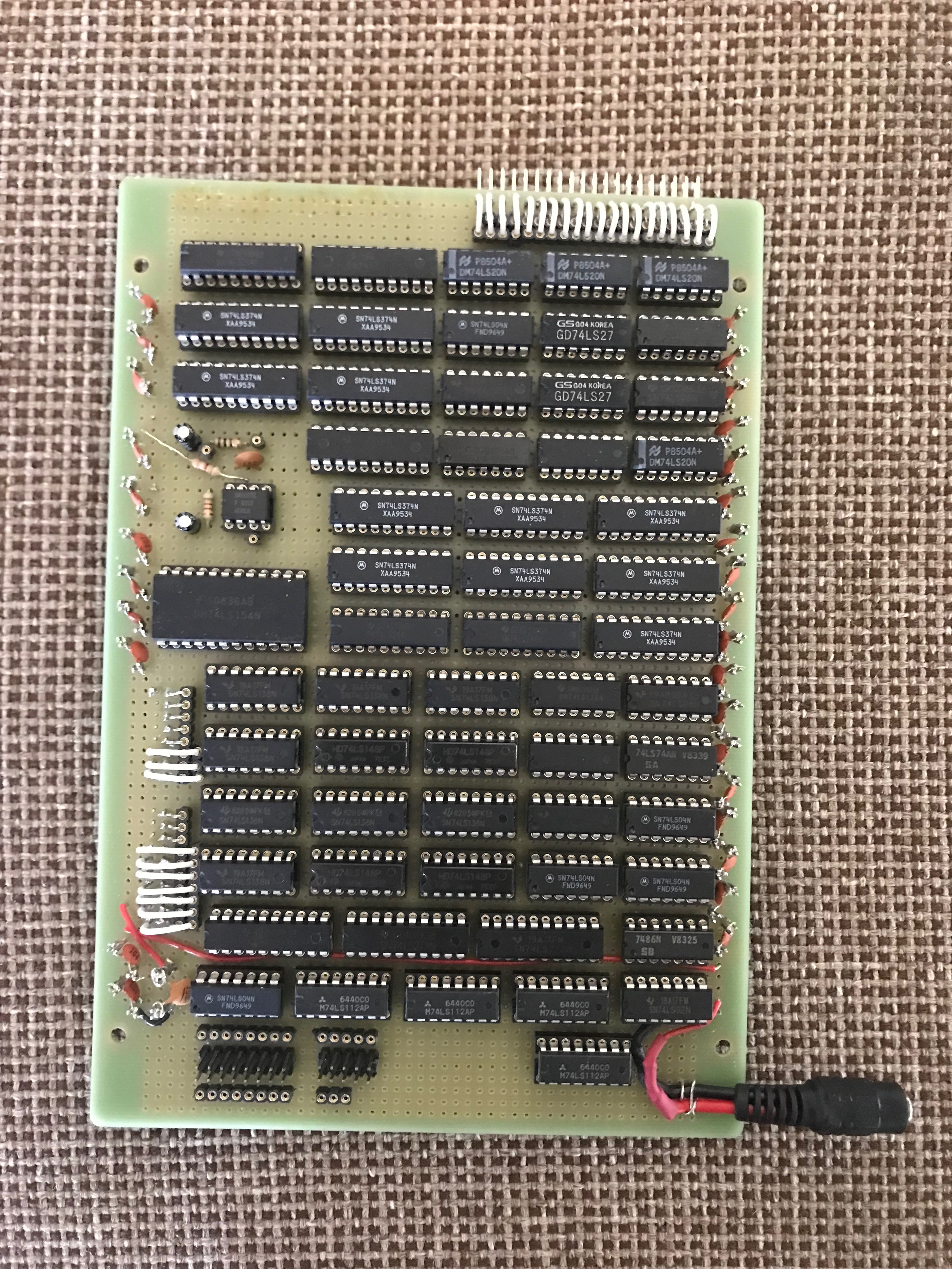
Now that the data is decoded, each of the value pairs are stored in an 8-bit register. There are 11 registers to store the 21 values. To display the values, a timing pulse is generated that loops through the registers one at a time, feeding the values into 4 LED driver chips. I originally tried to squeeze the logic into three random access ICM7228 chips. The logic proved too complex. Upon reflection, I decided it would be much easier to use the natural address values of the relay words which would require a fourth chip. During the pandemic these chips fell into the category of “out of stock and no estimate of availability”. The only chips that were available were older, obsolete serial access ICM7218 chips. The downside of these serial chips is that the display digit values need to be stored external to the chip. This is because each time a value changes, all the values need to be re-written serially.
The digit enable numbers and their chip assignments are shown in the table below. Note that some addresses are not used, but are required given the serial nature of the chips. Also note that the values need to go into the chip in reverse. The DE column shows the reverse numbering, i.e. the numbering from the Display Control 154 chip.
| RLYWD | Digit | Chip # | Enable # | DE |
|---|---|---|---|---|
| 0 | n/a | 2 | 28 | 7 |
| 0 | n/a | 1 | 18 | 7 |
| 1 | R3D5 | 2 | 27 | 6 |
| 1 | R3D4 | 1 | 17 | 6 |
| 2 | R3D3 | 2 | 26 | 5 |
| 2 | R3D2 | 1 | 16 | 5 |
| 3 | R3D1 | 2 | 25 | 4 |
| 3 | R2D5 | 1 | 15 | 4 |
| 4 | R2D4 | 2 | 24 | 3 |
| 4 | R2D3 | 1 | 14 | 3 |
| 5 | R2D2 | 2 | 23 | 2 |
| 5 | R2D1 | 1 | 13 | 2 |
| 6 | R1D5 | 2 | 22 | 1 |
| 6 | R1D4 | 1 | 12 | 1 |
| 7 | R1D3 | 2 | 21 | 0 |
| 7 | R1D2 | 1 | 11 | 0 |
| 8 | R1D1 | 4 | 48 | 15 |
| 8 | n/a | 3 | 38 | 15 |
| 9 | Noun2 | 4 | 47 | 14 |
| 9 | Noun1 | 3 | 37 | 14 |
| 10 | Verb2 | 4 | 46 | 13 |
| 10 | Verb1 | 3 | 36 | 13 |
| 11 | Prog2 | 4 | 45 | 12 |
| 11 | Prog1 | 3 | 35 | 12 |
| 12 | n/a | 4 | 44 | 11 |
| 12 | n/a | 3 | 34 | 11 |
| 13 | n/a | 4 | 43 | 10 |
| 13 | n/a | 3 | 33 | 10 |
| 14 | n/a | 4 | 42 | 9 |
| 14 | n/a | 3 | 32 | 9 |
| 15 | n/a | 4 | 41 | 8 |
| 15 | n/a | 3 | 31 | 8 |
These LED driver chips require 17 pulses to load them. The first write pulse sets the mode. Since this is the same value for each chip, one pulse will be applied to all four chips. The next 8 pulses set the first two chips data values and the following 8 pulses set the second two chips data values. This logic requires a 5-bit counter. Since there are many 4-bit counters, I chose to add a flip flop to be the fifth counter bit. Since not all the states are required and to take advantage of a single 4 to 16 bit decoder chip, I use the following states.
| State | Digit |
|---|---|
| 11110 | Start State |
| 11111 | Sent Mode |
| 00000 | First Data Value |
| ... | ... |
| 01111 | Last Data Value |
| 10000 | Stop Counting |
The OUTDAT pulse is as fast as 1 MHz which is much faster than the 2 Khz cycle timer to update the display and they are out of sync. To get them in sync one flip flop is used to capture the pulse. A second flip flop is then used to sync the signal. This is then used to start the counter and avoid a spurious write pulse. There are also two flip flops to represent the 5th bit of the counter. The first one captures the TC signal from the counter chip. The TC is set when all four bits are one. The next flip flop is set up as a toggle and toggles the next cycle, thereby changing to a one state when the counter goes to all zeros.
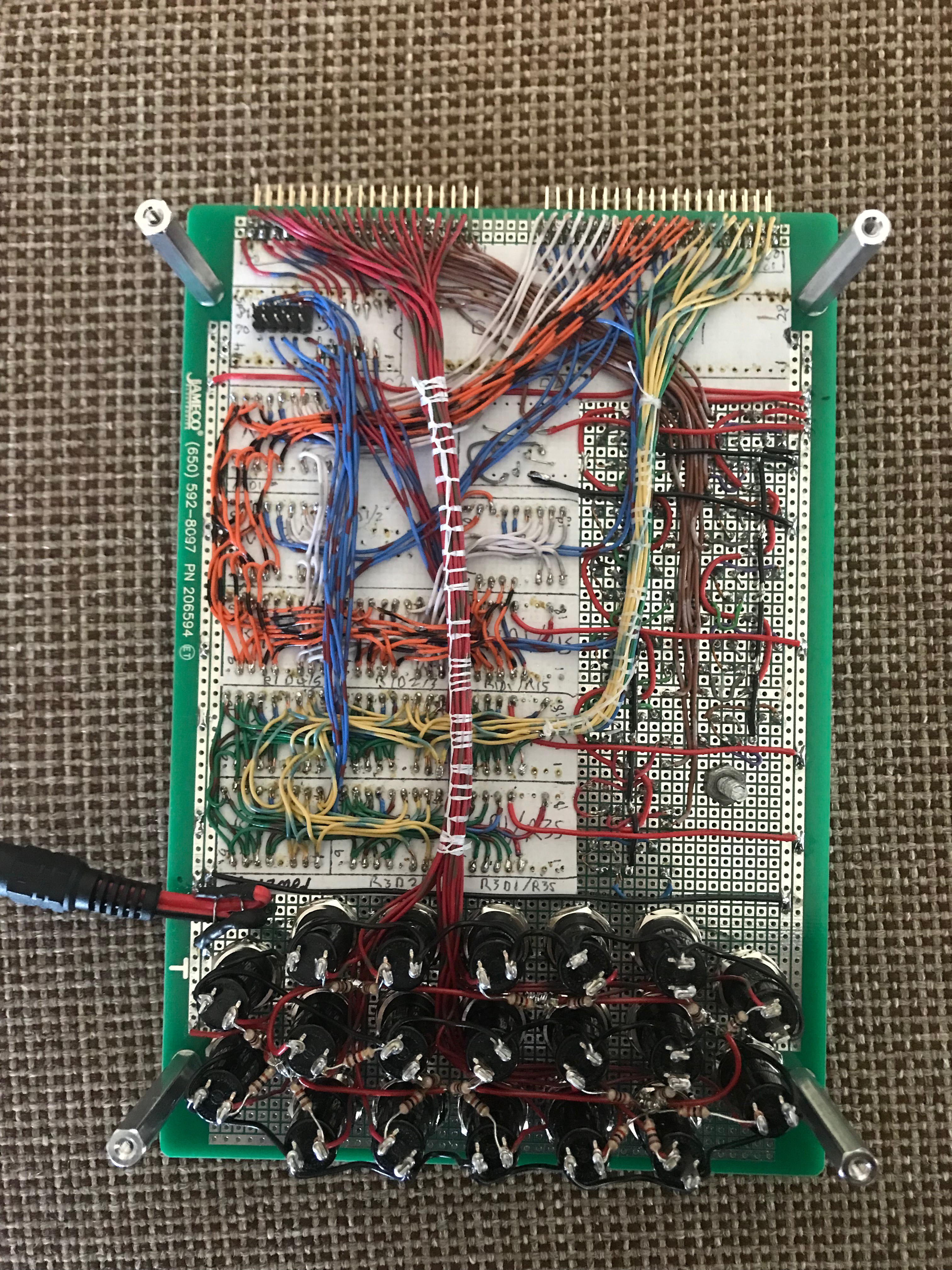
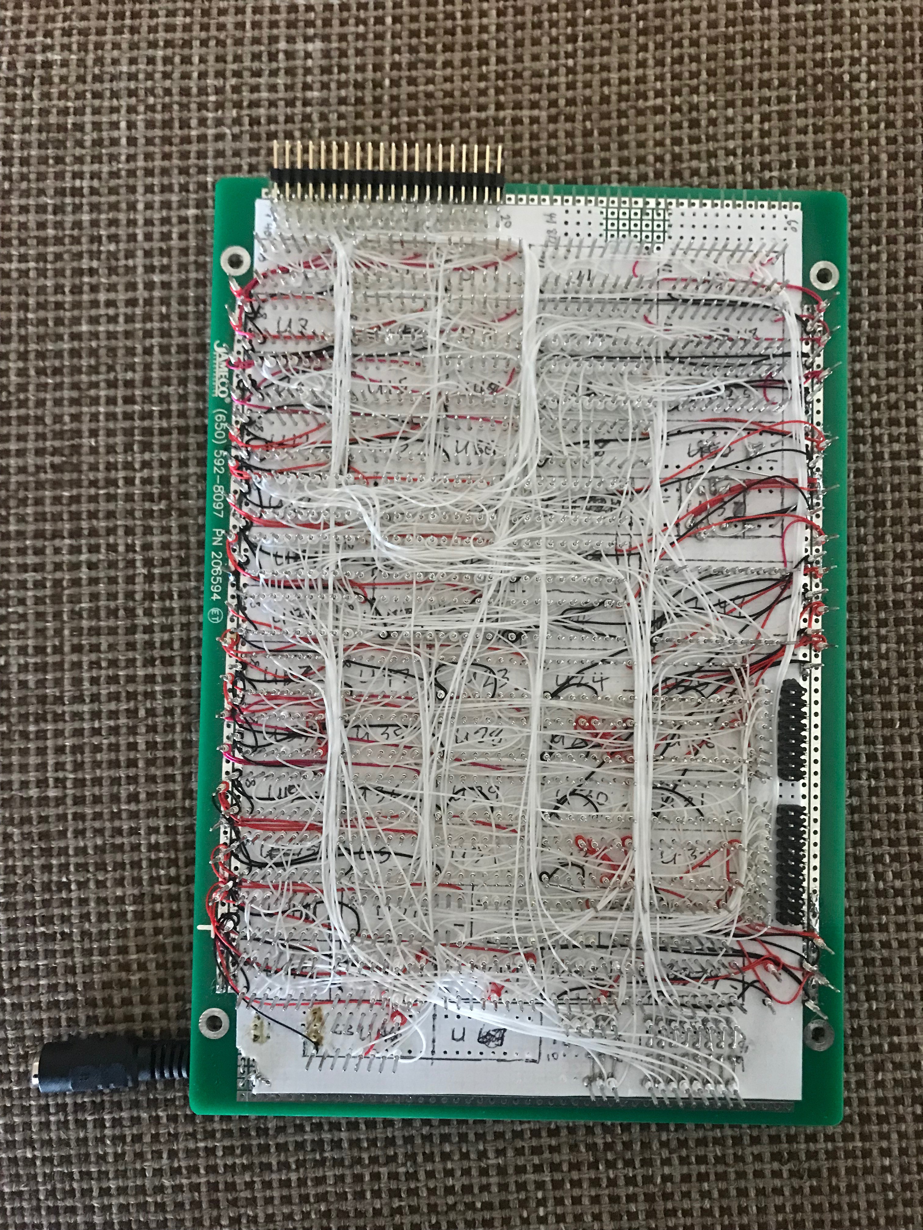
The DSKY consists of three boards. The front board is a solder board containing the astronaut facing keyboard, display and indicator lights. The middle board and back board are wire wrap boards. The middle board contains the four LED driver chips and the logic to drive the required data pulses. The back board is the majority of the logic.
Discussions
Become a Hackaday.io Member
Create an account to leave a comment. Already have an account? Log In.