 Guido
GuidoOverview
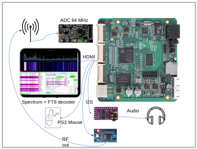
At the beginning the antenna is directly connected to the AD9226 Analog to digital converter, sampling at 64MHz. The 64MHz clock is generated by the FPGA, so that it can sample it well (more on this later)
Please note there's no external PC because the Zynq 7010 embeds a Dual Core Cortex A9 running Linux (Xilinx PetaLinux) in addition to its powerful FPGA.
- AM / SSB demodulated audio can be listened by headphone or loudspeaker
- Wideband or zoomed radio spectrum can be viewed on the screen
- demodulated FT8 can be viewed on screen and decoded using a WSJT-X adapted version
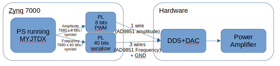
- modulated FT8 is sent to the Antenna
Similar projects
KiwiSDR is a very good example of a wideband 0-30 MHz FPGA based SDR receiver but it costs 450 Euro and it needs a BeagleBone computer.
Red Pitaya is a wonderful project with a lot of possibilities and it is open source but the board costs around 600 Euro.
Panoradio (https://panoradio-sdr.de/panoradio-sdr/) is much more than I'm trying to build (100 MHz spectrum, 16 bits samples) but its components (FPGA board, A/D board) are much more expensive as well.
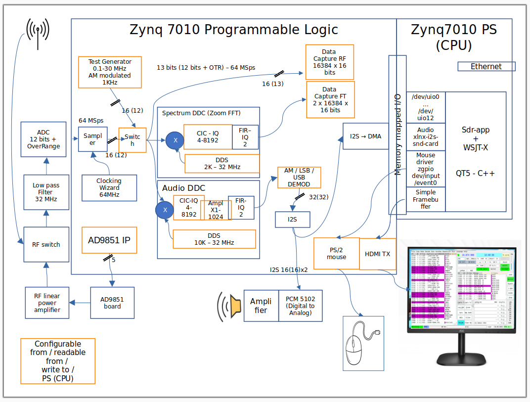
Block Diagram
At this time (Aug 2023) the whole design is pretty consolidated.
TODO:
- low pass 32 MHz
- RF Switch
- RF linear power amplifier
Numbers
All the number crunching in the fabric logic is perfomed with two's complement.
When I write xx(yy), e.g. 32(28), I mean that the numbers are 32 bit two's complement but the maximum expected value is
- 2^27 <= value <= 2^27-1
ADC - Analog to Digital Converter - AD9226
The board has no clock reference (see the AD9226 board schematic) and therefore the 64MHz clock must be supplied by the FPGA. In this way:
- the AD9226 outputs data on the dropping edge of the clock.
- the FPGA samples on the clock rising edge
See the picture below and for further details see the AD9226 datasheet from Analog Devices.
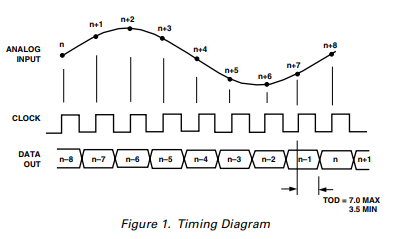
A concern is about the clock jitter coming from the FPGA. Will it add noise to the received signal?
For example, in this project ADC to DMA to Ethernet with a ZYNQ 7000, the sampling clock is generated outside the FPGA
FPGA
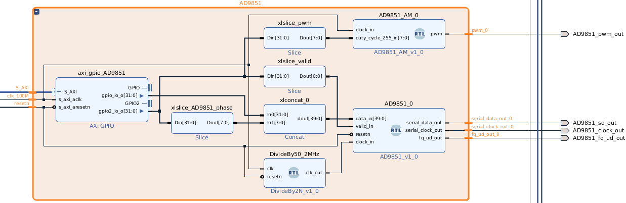
The functions operating in the FPGA are the following.
- It supplies a 64MHz clock to the AD9226 and receive 12 bit data + 1 bit "Over The Range" from it.
- An internal signal generator 0.1 - 30 MHz AM modulated at 1KHz can be be used for testing purposes.
- One "capture block" will capture 16384 samples (at 64MHz) at a time. These samples are sent to the FPGA PS and from there to the sdr-app (a QT5 C++ app running on the Zynq PS) to show the full 32 MHz radio spectrum and waterfall.
- One DDC (Digital Down Converters) with selectable bandwidth (10 MHz, 3 MHz, 1 MHz, 300KHz, 100 KHz, 30 KHz, 10 KHz,) will zoom the radio spectrum and waterfall with increased resolution.
- Another DDC can be tuned on a specific frequency to demodulate and decode e.g. the FT8 frequencies on 80 40 20 15 and 10 meters, with selectable (100KHz, 30KHz, 15KHz, 8KHz, 4KHz and 2KHz)
- It generates the TMDS signals to drive a DVI interface (HDMI without audio and control)
- It generates I2S signals to drive an external I2S DAC to listen to AM broadcasts and SSB radio hams
- It interfaces a PS2 mouse
Getting started with the EBAZ4205 board
The whole project is quite challenging, especially for those people who have never worked with Xilinx Zynq development environment (Vivado, Vitis, Petalinux). Therefore I strongly suggest to start with a "getting started" project. See my Hackaday project: EBAZ4205 development environment
The Analog Input
I didn't like that AD9226 12-BIT 65MSPS board attenuates the input signal by -8,4 dB. So I decided to modify it to get some amplification, using far more 12 bits ADC range.
I designed a circuit like this: ...
Read more »


 MS-Dzo
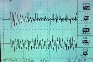
 Bruce Land
 zpekic
EBAZ4205_SDR is always 0404 Sorry..