 Dave Collins
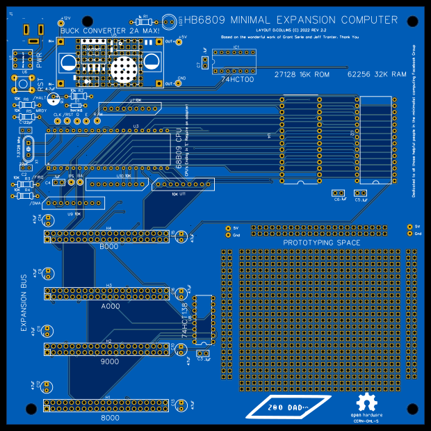
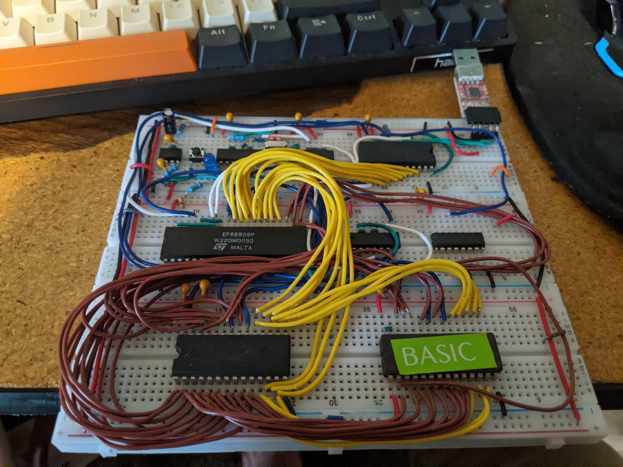
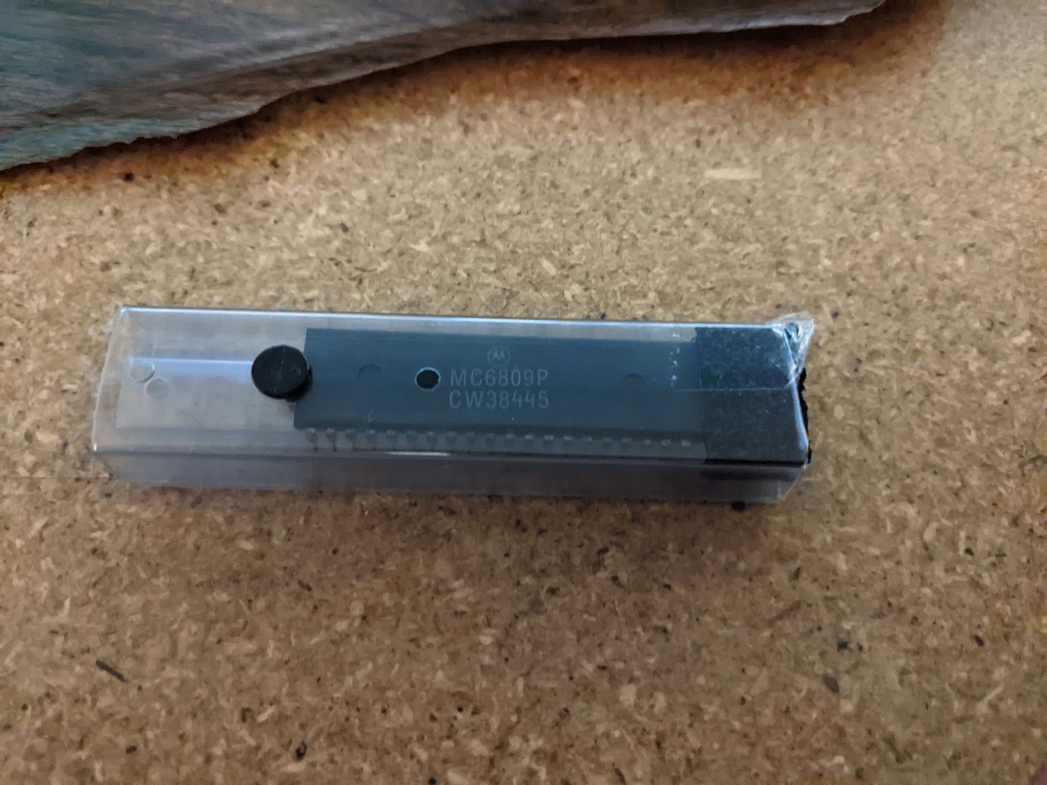
I wanted a low cost kit like computer based around the 6809, with a very simple expansion bus.
Design goals:
- Cost - try to keep board footprints small (this was hard, further minimization with surface mount parts would be the way to go even lower)
- Minimal - keep the focus on simplicity, very few chips and very simple memory map
- Extendable - break out as many test points as practical and in locations that make them easy to bodge to.
- Runs existing firmware - Since I plan to use this as a learning platform I want the computer to be built around a reference design
- Grant Searles Page : http://searle.x10host.com/6809/Simple6809.html
- Jeff Tranter's page : http://jefftranter.blogspot.com/2019/01/a-6809-single-board-computer.html
- Open hardware (CERN-OHL-P) -- a text copy is in the files section if this link is ever bad.
Liability / warranty language from the license
5.1 DISCLAIMER OF WARRANTY -- The Covered Source and any Products are provided 'as is' and any express or implied warranties, including, but not limited to, implied warranties of merchantability, of satisfactory quality, non-infringement of third party rights, and fitness for a particular purpose or use are disclaimed in respect of any Source or Product to the maximum extent permitted by law. The Licensor makes no representation that any Source or Product does not or will not infringe any patent, copyright, trade secret or other proprietary right. The entire risk as to the use, quality, and performance of any Source or Product shall be with You and not the Licensor. This disclaimer of warranty is an essential part of this Licence and a condition for the grant of any rights granted under this Licence.
5.2 EXCLUSION AND LIMITATION OF LIABILITY -- The Licensor shall, to the maximum extent permitted by law, have no liability for direct, indirect, special, incidental, consequential, exemplary, punitive or other damages of any character including, without limitation, procurement of substitute goods or services, loss of use, data or profits, or business interruption, however caused and on any theory of contract, warranty, tort (including negligence), product liability or otherwise, arising in any way in relation to the Covered Source, modified Covered Source and/or the Making or Conveyance of a Product, even if advised of the possibility of such damages, and You shall hold the Licensor(s) free and harmless from any liability, costs, damages, fees and expenses, including claims by third parties, in relation to such use.
Support the Project:

10% of your order will go back into covering the cost of prototyping, parts and other materials for creating new and interesting projects for me to write about. Including new modules for the HB6809
Launch Video:
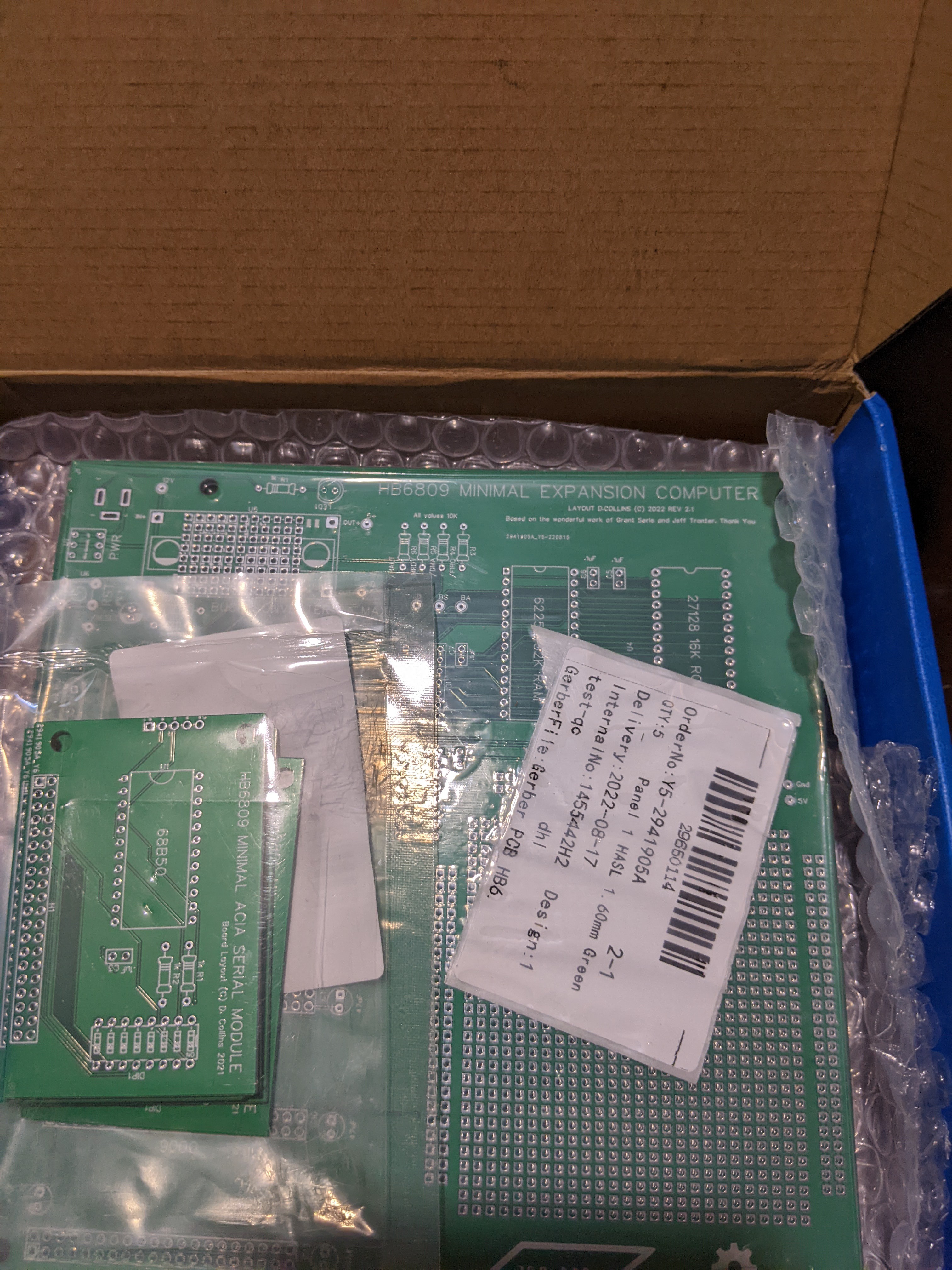
Build Files:
Github -- My Github for the HB6809
Build Recommendations:
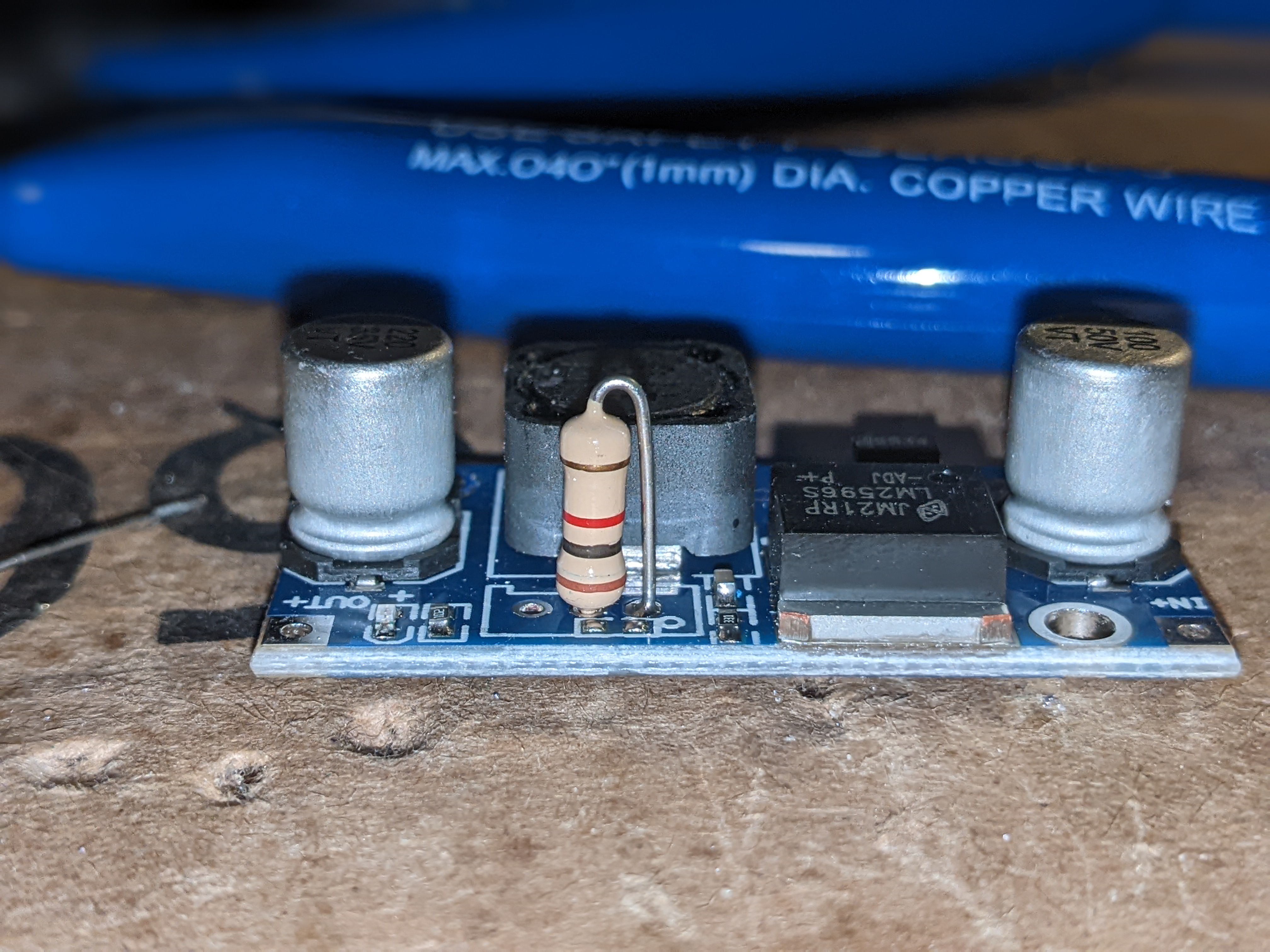
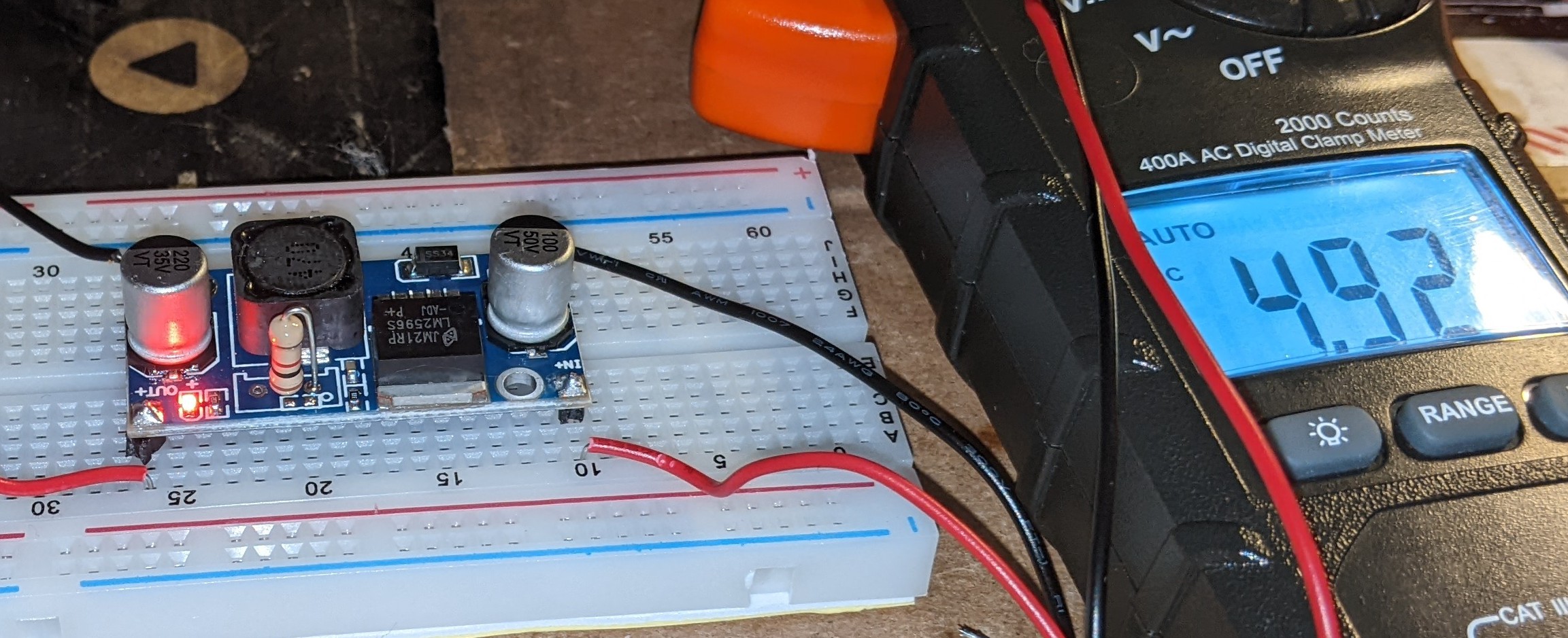
For the LM2596 DC to DC Converter module, It may be prudent to put break away pins (like used in a standard header ) on each of the four corners to prevent the module from shorting on the board. Additionally if you choose to remove the variable resistor from the module I found a standard through hole resistor (1K %5) provides a near perfect 4.9V you can simply mount it in the two holes that are laterally located next to the SMD pads that are revealed when you pull the variable trim pot from the board.
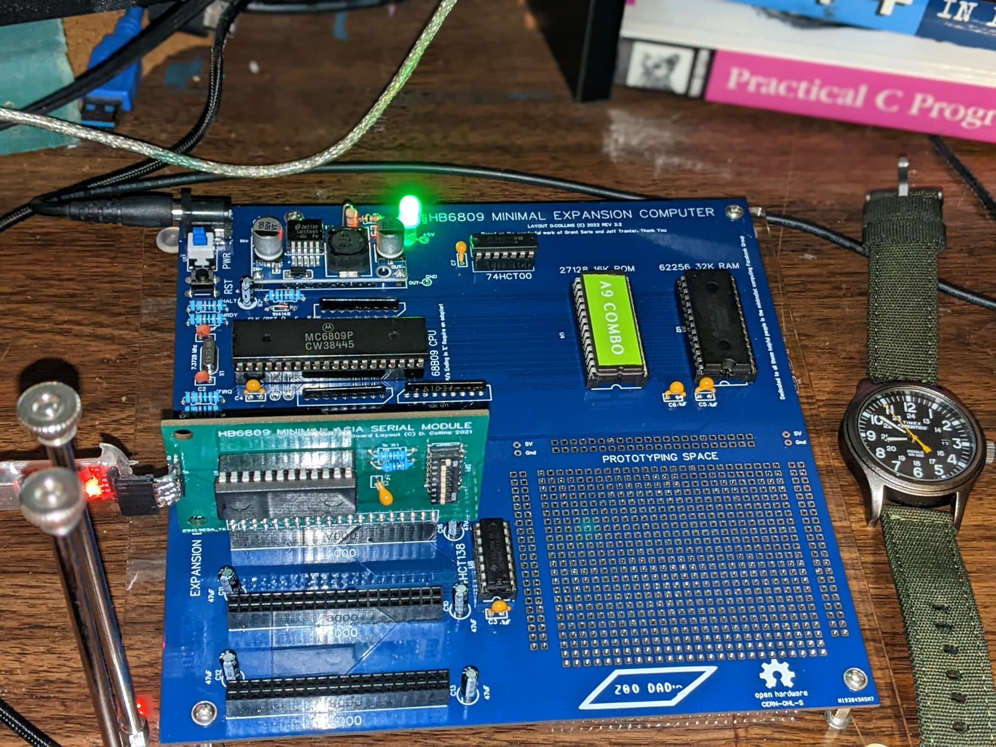
Optional power module mod:
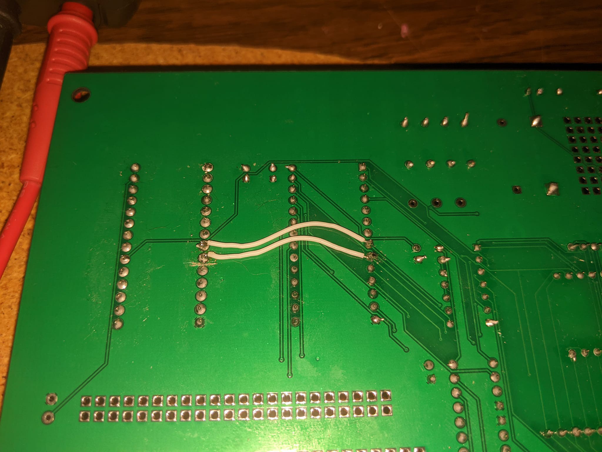
Stand offs installed to prevent board from shorting:
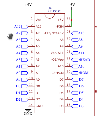
HCT vs LS considerations:
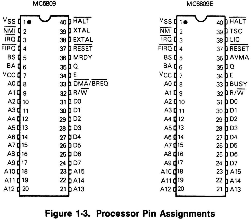
I've used HCT logic chips in my design, you can build this with LS, but the fan out implications are considerably more dire. particularly with the address decode lines being tied directly to the two 74 series chips. Pay particularly close attention to the 6809 datasheet in this area, remember, HCT gates draw considerably less current from the bus, and since these decode gates are directly connected to the bus this will change those...
Read more »


 Gee Bartlett
 Colin Maykish
 Anders Nielsen
A couple of thoughts:
1. 74ACT parts will give you more drive capability (and speed) than either HCT or LS.
2. I'm not sure why you're pulling up the address and data lines - U7, U10 and U11 can probably be eliminated.
OK, there's a third:
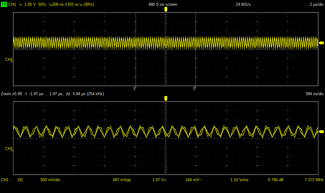
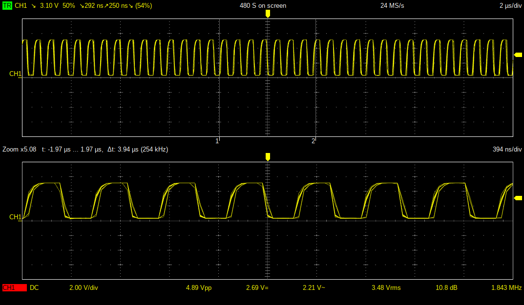
3. I wouldn't trust that buck converter & would add a crowbar circuit in case it fails in a bad way (passing the input voltage straight through to the output).