 Dave Collins
So it has been a long time since the last update, but here goes....
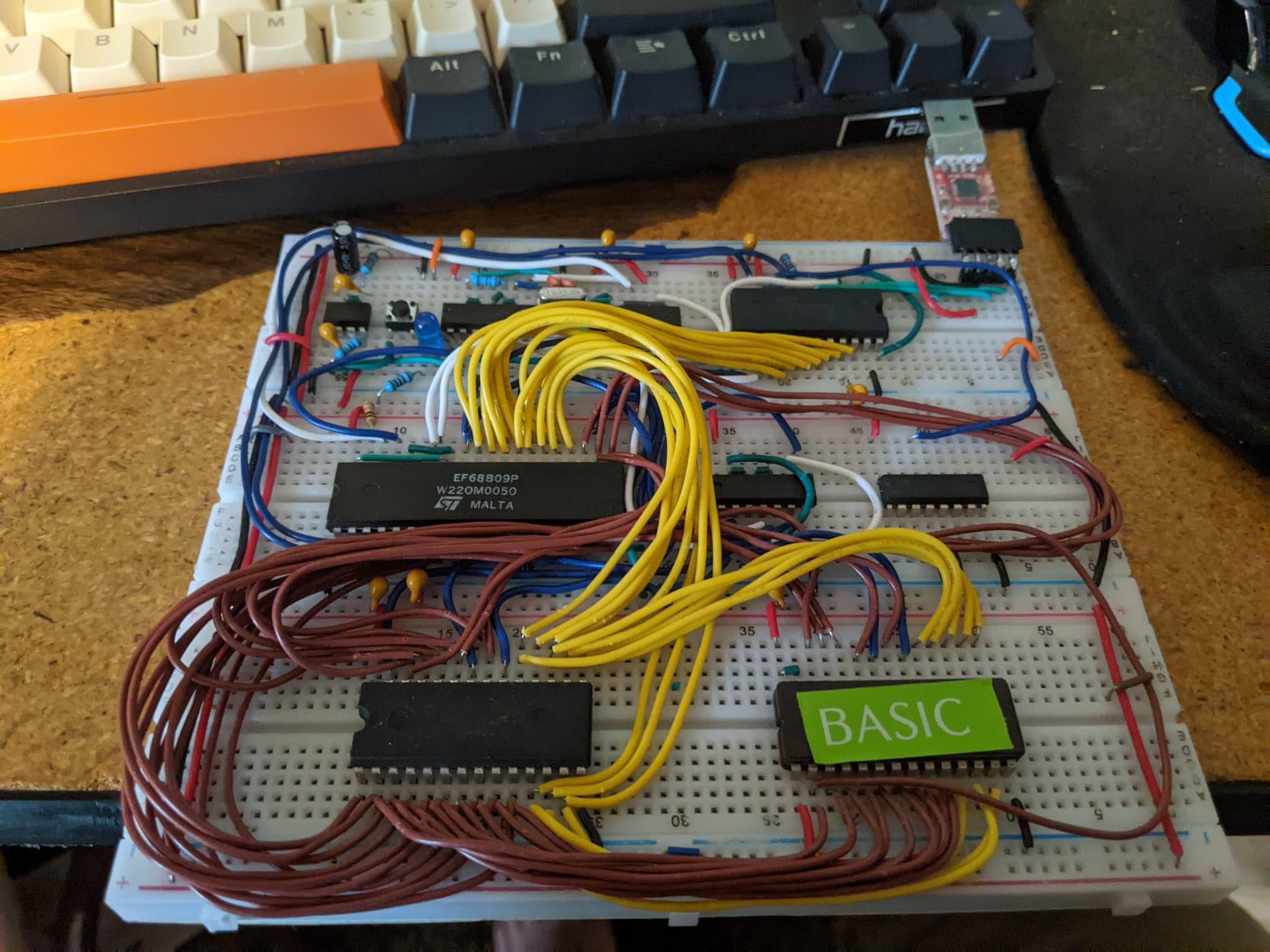
So I built up the Grant Searle / Jeff Tranter Single board 6809 computer on a breadboard:
If you haven't checked out the minimal 6809 on their sites its a good read both of them, and definitely more educational than anything you'll get from me!
I put together the reset / clock divider we talked about in my last update. Consequently, a lot of the schematics were poorly drawn in that update and so it's best to ignore them. It worked like a charm but like so many things I wound up simplifying further and just hooking the crystal up to the CPU directly (its built in to the chip and though I don't think anybody has de-capped a 6809 to check (that I know of?) It is VERY likely the clock is normalized with an inverter heading into clock generation inside the chip so why bother? In the end, being able to scale the chip clock was fun to be able to run the CPU at 1 MHz, but I was always going to put the vintage chip in my collection and simply use the early 2000's era Thompson / SGS Version any how; and it runs at 2 MHz.
Lets take a trip on down to feature creep city:
It really is the city where good projects go to die...
I knew about this issue (lets face it no good project is immune). I had an idea to learn a little bit about address decoding, and expansion busses. I decided I wanted a few things out of this computer build:
- I wanted it to be low cost ( not made of money, retro kits are expensive lets be real somebody has to pay for the time and energy that goes into making these things into kits, documenting them, distributing them etc.)
- This means I wanted to start with a open or very simple design and expand
- I wanted to add very few parts, again to keep the costs down.
- I wanted to learn about address decode, and busses the way I learn things by doing and making mistakes.
- I knew, and accepted it wasn't going to be perfect but I wanted it to at least work; and be smart and minimal so that as many people could try it out or expand on it like I expanded on the last two projects.
- I wanted the chip count to be low, and I wanted the chips to mainly be HCT again for cost reasons as well as availability (you can still get through hole HCT chips new, at generally reasonable prices.)
- I wanted there to be a PCB, and example expansion card PCB I could release as open hardware. I didn't feel right taking somebody else's design and hard work, and selling it as a kit to make money off of. (even if i was modifying it in a big way It still runs Jeff's firmware, witch is kind of grants firmware, Which is KIND OF Microsoft's firmware.) This is a clone, with bells and whistles and I am lucky to just have the community engagement in kind based off of the work of these two people.
- I wanted to focus on the 6809 and pin compatible 6309, I had no plans to directly support the external clock chip versions.
I set out to build a back plane. I had no idea what a rabbit hole this was going to be. First off lets be real, The world doesn't need another back plane standard for retro computers:
- STEbus
- Euro card
- S-100
- Z50 Bus
- even RC2014 (don't even get me started!)
this was a huge mistake. full stop.
I released several ideas for sub-par backplane designs, similar to RC-2014 and Z50 bus on some of the groups i frequent on Facebook and prepared for worst. The internet is a great place to get feedback, but its also frustrating for people like me who are learning, and might not get everything right all the time (how dare I right? ) Lets face it, its never any fun to be told that you have a terrible non-starter of an idea. But to be honest I rather appreciated it ... though it did do a number on my mental space for a few hours, I'll live this is how we learn.
I devised that I wasn't being true to my design goals. I let feedback drive the features (and thus the complexity to an astounding level.) by the time it was done I was supporting, or trying to support both clock types of the 6x09 family, all of the signals in the CPU and to be honest that was a HUGE Mistake.
Once I had time to think it over, I went with a more conservative design:
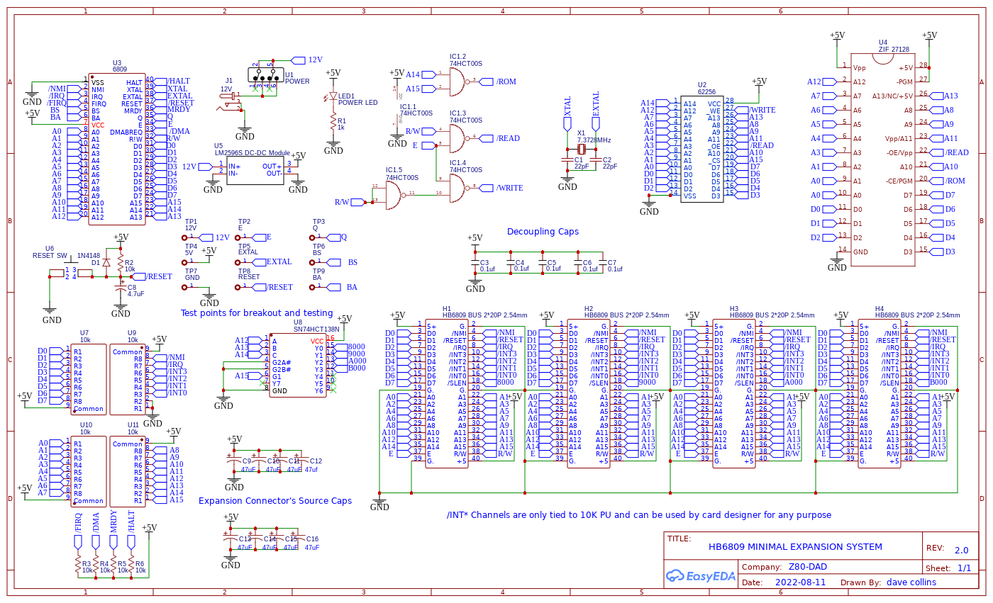
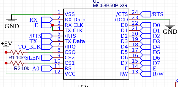
The expansion connector looks like this:
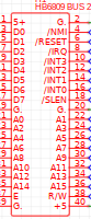
As you can see this is not a full signal expansion bus, this is simply the address bus, the data bus, the main interrupt, the E clock the R/W signal, a select line (/SLEN), and 4 interrupt channels that only interconnect the 4 slots. The more signals you add the more complex and demanding your connector design has to be. This is truly a minimal what you see is what you get expansion port. I'd not go so far as to say it's an expansion bus, but it has bus like tendencies. If it helps, think of it as a C64 expansion port, except there are 3 of them and they are addressed. The over all expectation is that this will work (or should work) at 2 MHz no problem... I don't know if it will worked with an overclocked 6309 at 5 Mhz with a 20 Mhz starting clock, this would require much more attention to ringing in the signal lines than what I've done here... but obviously its wrong not to try right?
I used a standard (substandard?) 2x20 pin connector. The main board side is female, the card edge is right angle male. As you can see, an idea from comments in one of my posts I laid out the power and grounds so it is impossible to plug the card in and reverse power and ground (the result won't work but at worse it will mess up the address, and data bus lines).
The 4 interrupt channels are for if I decide to build a priority interrupt controller, they are tied high at the bus termination and they go between the cards so that you can pass off interrupts to the other slots to be maintained by a separate interrupt controller. Since they are handy, you could use one of them by simply bodging the broken out test points from the un-routed CPU signals if needed or use it for some other operation between the cards, so long as it is a normal TTL signal it should work.
The changes I did make:
I expanded the memory map slightly, added address decoding to expand the memory map to four 4k blocks, instead of 2 blocks which were minimally addressed. To keep things as simple as possible, and to further simplify the expansions, the address decoding is locked to the slots.
Grant's / Jeff's Memory map are as follows:
0000-7FFF -- 32K RAM
8000-9FFF -- FREE ADDRESS SPACE
A000-BFFF -- ACIA (minimally decoded)
C000-FFFF -- ROM SPACE
The HB6809 memory map:
0000-7FFF -- 32K RAM
8000-8FFF -- 4k free space
9000-9FFF -- 4k free space
A000-AFFF -- 4k free space (ACIA for Jeff/Grants Firmware to work unmodified)
B000-BFFF -- 4k free space
C000-FFFF -- 16K ROM
This is done by simply adding a 74HCT138 to decode the top four address lines in this manor:
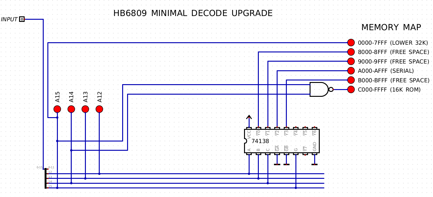
as you can see, the NAND gate is already in place from the previous designs, so this upgrade is fairly trivial, simply adding the chip. The only wiring change that needs to be done, is changing the ACIA wiring to pull the non-inverting enable pins high (CS0, CS1):
I tested these connections out on the breadboard and everything works:
Additionally I added provisions to the board for a very common buck converter module. It contains all of the glue bits, and the LM2596 switching regulator. There is a really good write up on its output characteristics here.
Here it is pictured:
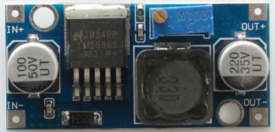
The ripple that is advertised on these modules is grossly underestimated, actual is closer to 200mVpp. Additionally the regulator does not hit unsafe heat levels at 1A, but would absolutely cook itself running at the advertised 3A! I recommend not running the regulator much past 1A but, if 2A is needed a heat sink and proper case ventilation are an absolute must. I installed the regulator on the breadboard build and found that the whole initial build on the breadboard never reaches anywhere near 1A. In fact actually only 225mA. This means technically it will run off of the 500mA supply provided by my USB to TTL converter, but as the final build has some expansion I felt the switching regulator was a must. As I am still waiting on PCB's I haven't done amp draw on everything as it would be including the interface card, I can only guess at 230mA is probably fairly close. When I did the layout I included a small prototyping space below the area where the module is mounted, allowing for air flow, as well as an option to build up a switching regulator or to use a compact regulator if that is the choice of the builder.
The layout:
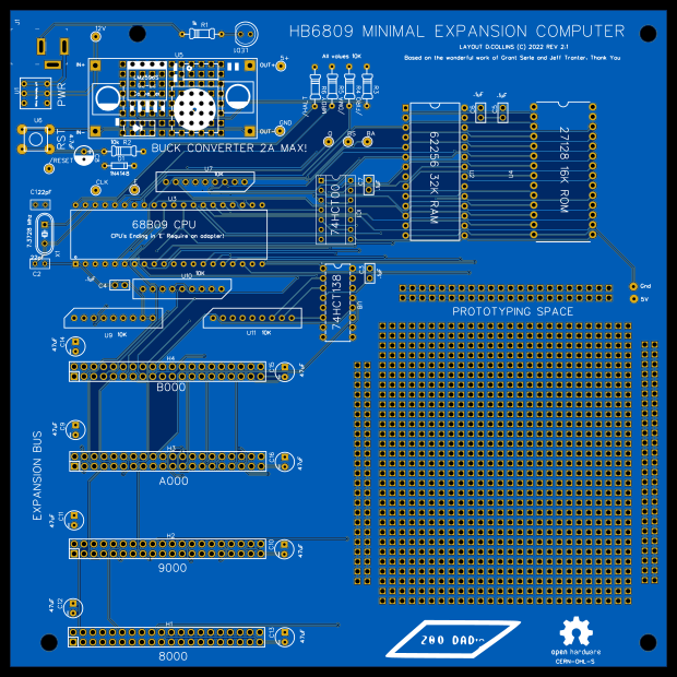
So this thing is truly a labor of love. I wanted to initially try to keep the build size on all of the cards to be sub 100 mm x 100 mm, however I couldn't make all of the slots fit in a usable configuration along with the CPU and ram so I ended up pushing the board size out to 160 mm x 160 mm (mini ITX). The bottom slot (H8000) Just fit in front of the 1 allowed expansion card space for that form factor. The remaining slots fall in line with the IO shield section of the board; and so would need to have their IO brought out to the shield if this were to be put into a case.
If there is interest, maybe I will make a mini-frame, with a CPU/ROM/RAM card to get the cost down further. The increased size means the board cost is around 15 dollars + shipping from china. I did not check the US based rapid turn prototype places, so that might be an option if somebody is interested.
I pulled all of the routed signals out on test points, or to pull up resistors for easy access if somebody needed to bodge in an extra route to one of the /INT* signals on the expansion slots. I added useful test points for the system clock, E, /RESET and all of the power rails. I was careful to allow for a rather large ZIF slot for the option ROM, so that swapping it out can be trivial if somebody would like to use one. Lastly I included a large prototyping space, more than large enough to build whatever expansion you have in mind; it's close to both the address decode logic and the slots so bringing over a select line is trivial. I built power rails on three sides of the area, and brought +5v and GND test points out near the prototyping area so these can be activated in any way you see fit.
I also built a small ACIA card:
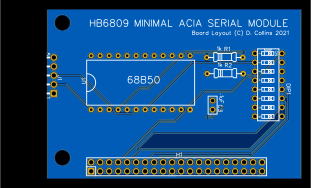
I put a set of DIP switches on there, to set the interrupt channel if desired, as well as the ability to route the interrupt line directly to the CPU.
Conclusion:
Hopefully, the PCB's will arrive soon and I can start building this thing up. Its safe to assume I am excited to get started! Inevitably its almost assured somebody will want to know the build cost. The PCB's were around 50 dollars shipped from china, this is likely the highest cost -- if you are building one of these up it would be in your interest to find a friend with a board or go together on shipping to keep the cost low. I did not check the US board makers, the costs are typically higher (with lower shipping cost). The passives including the crystal I had on hand but I estimate the cost for passives at less than 2 dollars if you pay for low cost shipping, or can bundle them with the rest of the chips. The logic chips were 2-3 dollars. The CPU and ACIA are around 5-9 dollars a piece, get them both from Jameco so that you are assured non-fake parts (usually). The RAM and ROM were 3-5 dollars each, the connectors are likely the largest parts cost; I have not priced them out yet but even using a standard 40 pin connector (that is on every raspberry pie ever made), I wouldn't be surprised if it wasn't 15 dollars for connectors and the regulator board. Given a lot of us seem to have some of this stuff kicking around already, it might be easy to get the build cost WAY under 100 dollars if you are careful how you go about it. Another thought, there is no reason you can't build this to use all CMOS parts using the 63c09, though you might need to change the firmware in order to get it into compatibility mode.
Discussions
Become a Hackaday.io Member
Create an account to leave a comment. Already have an account? Log In.
Nice work! And that CRT terminal is very cool.
Are you sure? yes | no
Yeah I love that for screenshots :) I can't get color to work very well in it if I could that would be my every day terminal but most of the time I use PuTTY. Thanks for your kind words:)
Are you sure? yes | no