 Wilfried Klaas
Nun geht's an die Software und das ist gar nicht mal so einfach. Zwar gibt es viele Beispiele auch für den 6502 mit 6522, aber von den Beispielen habe ich keines zum Laufen bekommen. Also musste ich selbst forschen. Zum Umschalten des Displays in den 4-Bit Modus muss ein gewisse Muster eingehalten werden. Und nebenbei machte dann auch das Display bei erneutem Reset Druck plötzlich mucken. Also muss das Display auch per Software einen Reset ausführen. Ließt man dazu das Kapitel im Datenblatt, erhält man eine genaue Reihenfolge wie welche Befehle mit welchen Zeitabständen erfolgen müssen. Dazu braucht man dann auch eine zuverlässige Delay Routine. Gleichzeitig habe ich nun auch ein paar zusätzliche Methoden zur Ausgabe ins ROM integriert.
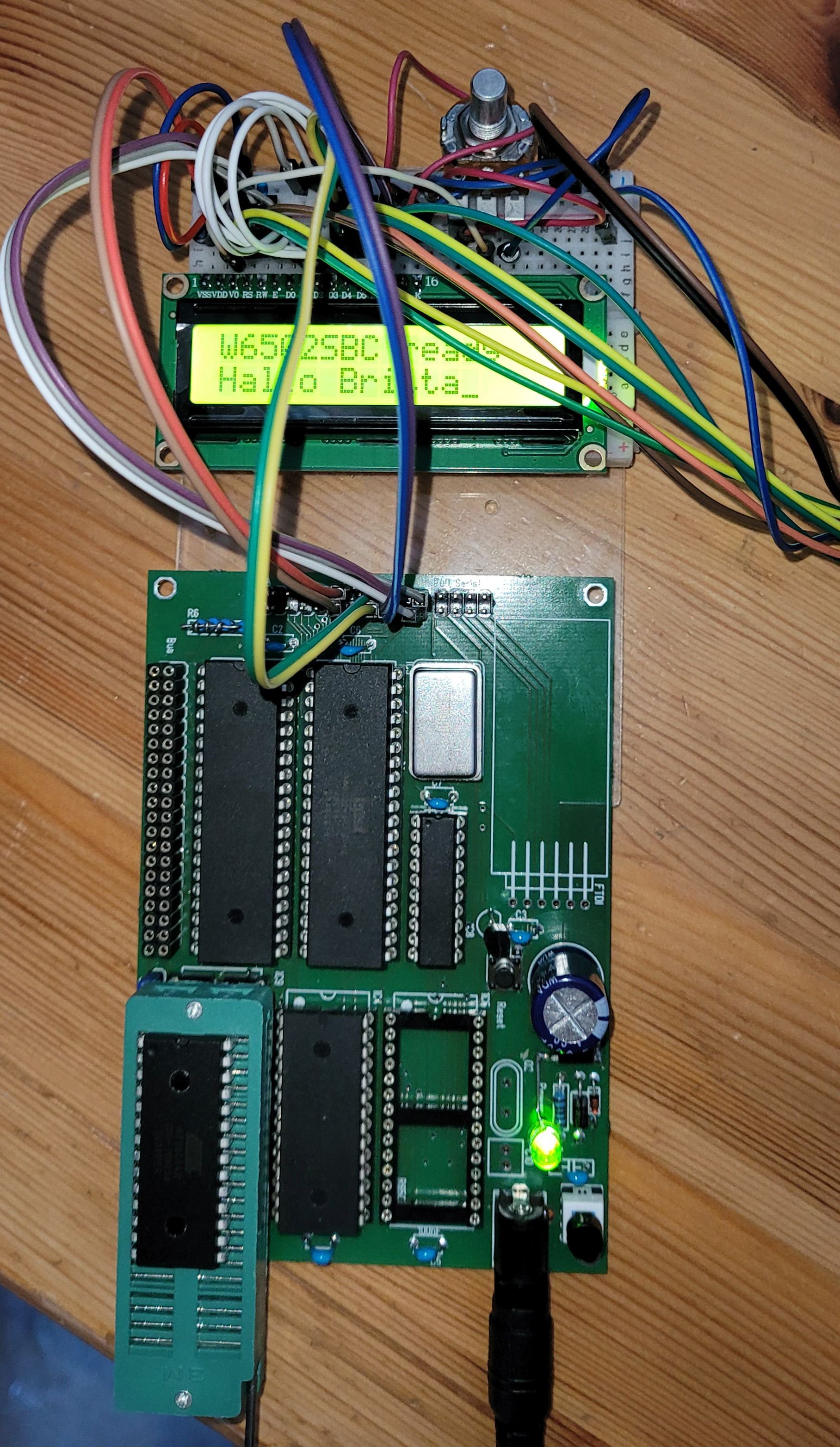
Nebenbei habe ich auch den ROM Sockel mit einem ZIF Aufsatz versehen. Das macht das Programmieren erheblich einfacher und schont die Beine der ICs und den Sockel. Evtl. muss ich auch mal über eine In-Circut-Programmiermöglichkeit nachdenken. Achja, die zusätzlichen Kabel, die vom Display nach recht weggehen, hängen an meinem Logic Analyser. Der hat mir dismal bei der Analyse und Programmierung sehr gute Dienste geleistet.
Hier die LCD-Routinen aus meinem BIOS.
; constants for LCD
LCD_E  .equ %10000000
LCD_RW .equ %01000000
LCD_RS .equ %00100000

;----- macros -----
.macro msg_out(msg)
  lda #>msg
  ldx #<msg
  jsr do_strout
.endmacro
;----- bios start code -----
do_reset: ; bios reset routine
  sei
  ldx #$ff ; set the stack pointer
  txs

  jsr do_ioinit  ; initialise port A an timer of VIA
  jsr do_scinit

  ;jsr lcd_clear
  msg_out(message_w6502sbc)
...
; ---- Display routines ----
do_scinit:    ; initialise LC-Display on port B
  ; D4..D7 on Port pins PB0..3
  ; RS; R/W and E on Port pins PB5, PB6, PB7
  lda #$ff   ; Set all pins on port B to output
  sta VIA_DDRB
  lda #0    ; all pins low
  sta VIA_ORB

  ; reset the display, wait at least 15ms
  lda #$58
  jsr do_delay

  ; send 3 times the reset...
  lda #(%00000011 | LCD_E) ; 1. RESET
  sta VIA_ORB
  eor #LCD_E
  sta VIA_ORB
  lda #$1f
  jsr do_delay

  lda #(%00000011 | LCD_E) ; 2. RESET
  sta VIA_ORB
  eor #LCD_E
  sta VIA_ORB
  lda #$01
  jsr do_delay

  lda #(%00000011 | LCD_E) ; 3. RESET
  sta VIA_ORB
  eor #LCD_E
  sta VIA_ORB
  lda #$01
  jsr do_delay

  lda #(%00000010 | LCD_E) ; Set 4-bit mode;
  sta VIA_ORB
  eor #LCD_E
  sta VIA_ORB
  lda #$01
  jsr do_delay

  ; after this command we can use the 4-Bit mode and we could use busy flag for former sync
  lda #%00101000 ; 2-line display; 5x8 font
  jsr lcd_instruction

  lda #%00001110 ; Display on; cursor on; blink off
  jsr lcd_instruction

  lda #%00000110 ; Increment and shift cursor; don't shift display
  jsr lcd_instruction

  lda #%00000010 ; Return home
  jsr lcd_instruction

  lda #%00000001 ; Clear display
  jsr lcd_instruction
  rts

lcd_wait: ; wait until the LCD is not busy
  pha
  lda #%11110000 ;set PORTB pins 0 - 3 as input
  sta VIA_DDRB
@lcdbusy:
  lda #LCD_RW
  sta VIA_ORB
  ora #LCD_E
  sta VIA_ORB
  ; loding high nibble with busy flag
  lda VIA_ORB
  sta HNIBBLE
  lda #LCD_RW
  sta VIA_ORB
  ora #LCD_E
  sta VIA_ORB
  ; getting the low nibble, address counter
  lda VIA_ORB
  sta LNIBBLE
  lda #LCD_RW
  sta VIA_ORB
  lda HNIBBLE
  and #%00001000 ; mask the busy flag
  bne @lcdbusy
  lda #$FF ; setting port to output again
  sta VIA_DDRB
  pla
  rts

lcd_instruction: ; sending A as an instruction to LCD
  pha
  pha
  lsr
  lsr
  lsr
  lsr
  ora #LCD_E
  sta VIA_ORB
  eor #LCD_E
  sta VIA_ORB
  pla
  and #$0f
  ora #LCD_E
  sta VIA_ORB
  eor #LCD_E
  sta VIA_ORB
  pla
  rts

lcd_secondrow: ; move cursor to second row
  pha
  ;jsr lcd_wait
  lda #%10000000 + $40
  jsr lcd_instruction
  pla
  rts
lcd_home:; move cursor to first row
  pha
  ;jsr lcd_wait
  lda #%10000000 + $00
  jsr lcd_instruction
  pla
  rts
lcd_clear: ; clear entire LCD
  pha
  ;jsr lcd_wait
  lda #$00000001 ; Clear display
  jsr lcd_instruction
  pla
  rts

do_strout: ; output string, address of text hi: A, lo: X
  phy
  stx TEMP_VEC
  sta TEMP_VEC+1
  ldy #0
strprint:
  lda (TEMP_VEC),y
  beq strreturn
  jsr do_chrout
  iny
  jmp strprint
strreturn:
  ply
  rts

do_chrout: ; output a single char to LCD, char in A
  jsr lcd_wait
  pha
  ; sending high nibble
  lsr
  lsr
  lsr
  lsr
  ora #(LCD_RS | LCD_E)
  sta VIA_ORB
  eor #LCD_E
  sta VIA_ORB

  pla
  and #$0F
  ora #(LCD_RS | LCD_E)
  sta VIA_ORB
  eor #LCD_E
  sta VIA_ORB
  rts

;------------------------------------------------------------------------------
; The count of outloops will be used from A.
; for 1MHz we had a cycle with 1us. if A = 1 we had 20 + 20 clks, which means a minimum of 200us,
; but the reality is somtime different. To get the 200us on my sbc there must be 32 inner loops.
; $01 = 200uS, $02= 360us, $04= 700uS, $08= 1,4ms, $10= 2,7ms, $20= 5,3ms, $40= 10,6ms, $80= 21,3ms, $FF=42,3ms
do_delay:
  phy     ; 3 clk
@outer:
  ldy  #$20  ; 2 clk, this gives an inner loop of 5 cycles x 20 =  100uS
@inner:
  dey     ; 2 clk
  bne @inner  ; 2 + 1 clk (for the jump back)
  sbc #$01   ; 2 clk
  bne @outer  ; 2 + 1 clk exit when COUNTER is less than 0
  ply     ; 4 clk
  rts     ; 6 clk
Discussions
Become a Hackaday.io Member
Create an account to leave a comment. Already have an account? Log In.