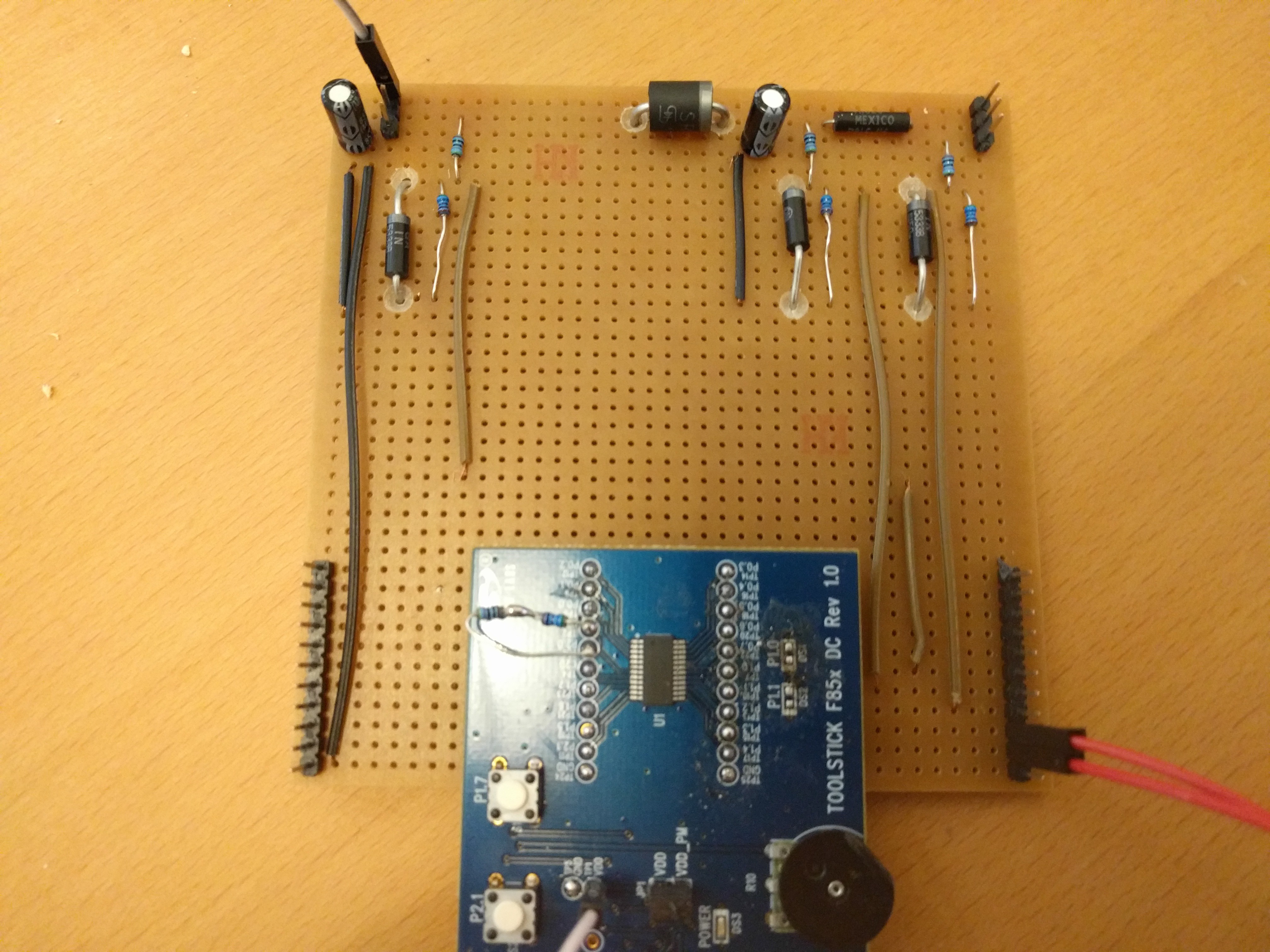
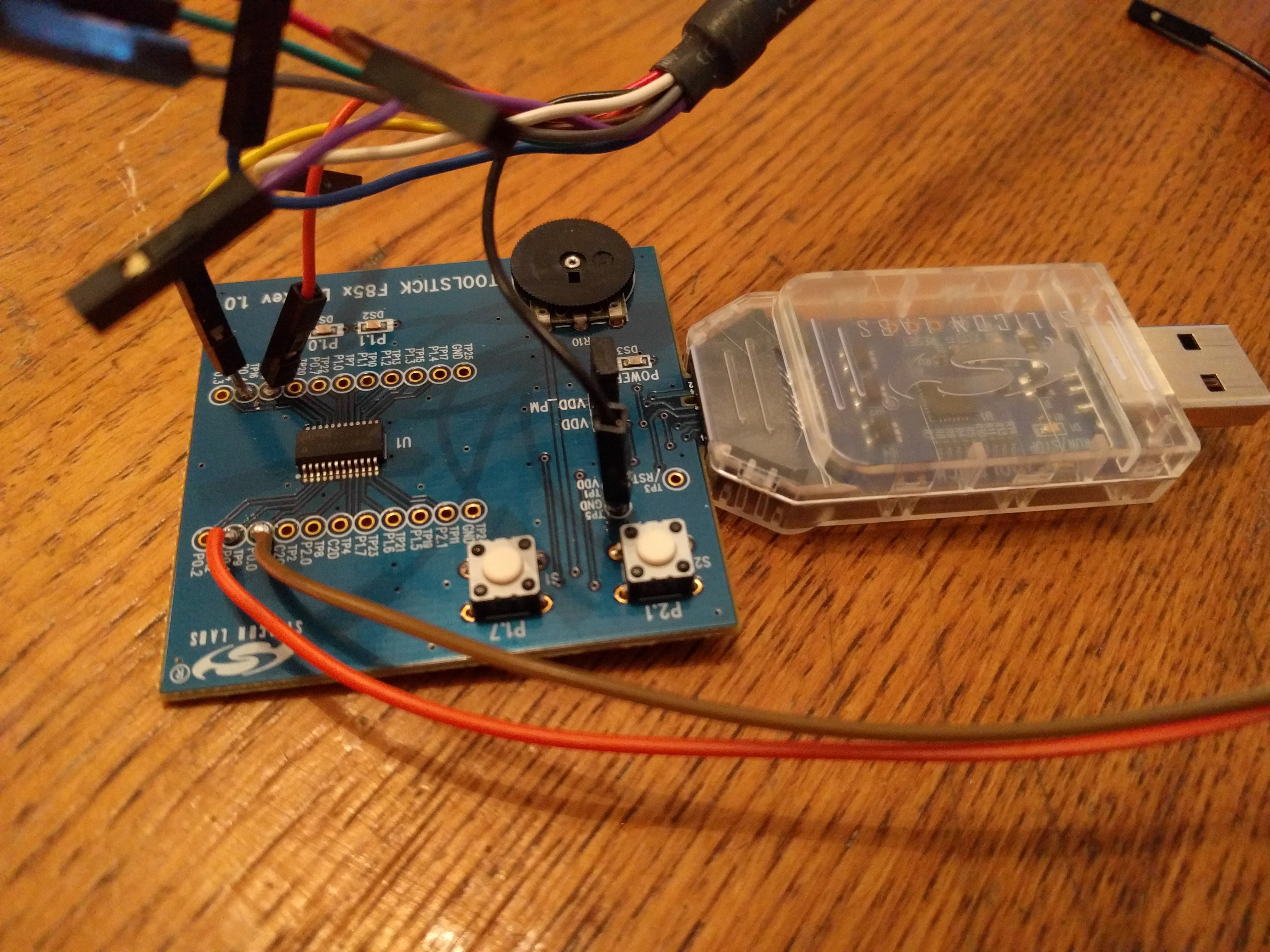
Close
0%
0%

Switcher

A switch mode power supply controlled by an 8051 processor.

Similar projects worth following

Architecture: 8051

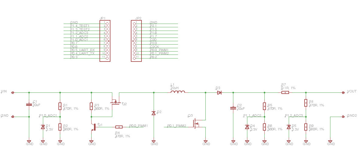
Microcontroller: Silicon Labs C8051F850-C-GU

Toolchain: Keil c51*

The 8051 processor is a popular architecture and Keil provide a comprehensive development environment allowing for simulation and in-system debug.

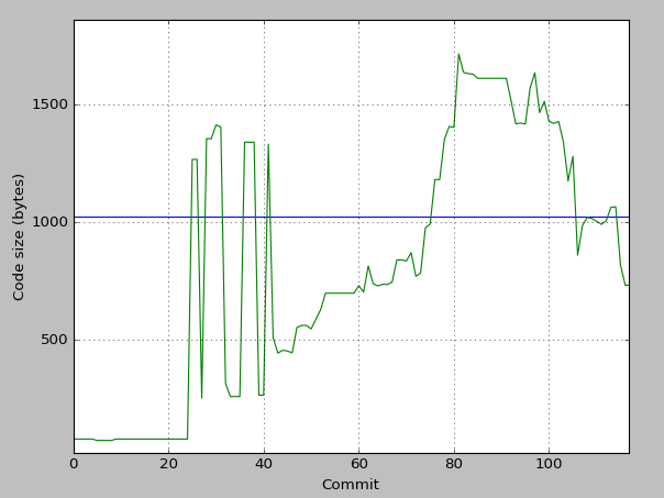
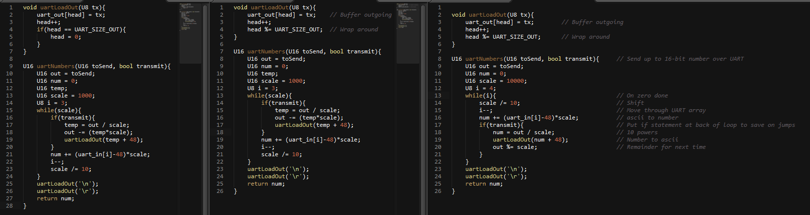
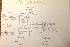
The approach is to implement a feature, optimise code size as much as possible and if it fits in less than 1KB repeat. At present these features include...

  1. Enable UART for debug
  2. Enable ADC
  3. Enable PWM
  4. Control PWM duty cycle from ADC input
  5. Implement PID controller
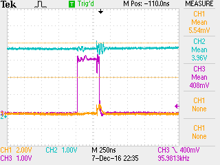
  6. Working boost convertor
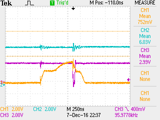
  7. Working buck-boost convertor
  8. Implement constant current mode
  9. Digital (UART/SPI) interface for user to control voltage/current
  10. Change diodes to FETs switched by the microcontroller to improve efficiency

* The compiler limits machine code generation to 2KB (not a problem) however it also limits the use of memory less than 2KB by always jumping to address 0x0800 and then continuing with compiled assembler.

Adobe Portable Document Format - 4.40 MB - 01/04/2017 at 21:19

Preview
Download

  • Final log

    Ashley Robinson01/04/2017 at 21:33 0 comments

    Project entry:

    Along with hackaday logs on the project page...

    The project is summed up by the following document (including build instructions, BoM, etc): Switcher.pdf

    The hardware and software is available in the github repo: https://github.com/ashleyjr/Switcher

    The final project meets the 1KB criteria and majority of the project goals have be achieved.

    Personal reflection:

    My knowledge of switch mode power supplies was already fairly complete but I tend to use off the shelf controllers which, when treated with respect, are quite simple to get up and running. I chose to develop a SMPS from scratch as a way of putting myself in design position of a commonly used component so that I might better understand why they behave as they do.

    Using the Keil c51 compiler and diving deep in to the assembler was a valuable experience. I often tend to avoid assembly like the plague but monitoring the code size byte by byte has taught me subtle changes in C can make huge changes in the assembler. I also have a greater appreciation of the 8051 architecture and can understand why new chips based on the this design are still entering the market.

  • Code size analysis

    Ashley Robinson12/31/2016 at 17:16 0 comments

    As a quick aside I wrote a small script to plot the code size produced against commits. Initial development is erratic, the size slowly grows as more features are added and eventually I keep optimising the code to get back below the limit.

  • Optimisation

    Ashley Robinson12/31/2016 at 01:30 0 comments

    The functionality of the project almost complete code must be optimised to reach the target of 1024 bytes or less.

    In this example the two functions under inspection regard UART traffic. One to load the buffer which is unloaded from a timer and the second is used to move data between an unsigned 16-bit integer and ASCII representation of that number. Working from left to right in the image below the code size improvement is as follows...

    1. 1021 bytes
    2. 1016 bytes
    3. 1004 bytes

    The first step replaces an if statement with a modulus operation to control wrap around of the UART buffer. The second step shifts an if statement to the end of a loop to reduce the number of jump operations the compiler generates.

    The more bytes than can be removed from the generated assembly will enable more options to be placed in the UART menu structure. Similar techniques will be used to reduce code size where possible.

  • Controller first steps

    Ashley Robinson12/14/2016 at 23:43 0 comments

    The controller has been implemented using only proportional and integral control. The derivative control likely not be required Below is a graph of output voltage of the switcher with increasing input voltages. Under minimal load this will need to be tuned to respond appropriately for give step sizes and output loads.

    The ability to switch the output voltage on and off is given by the menu. Two commands are available to enabled and disable the switcher. This along with the PID controller itself has pushed the project over the 1KB limit.

  • Hardware build part 2

    Ashley Robinson12/07/2016 at 23:30 0 comments

    The additional switching components have added to the stripboard . Using only the small load from the potential dividers on the output (500R) the capabilities have been tested in open loop mode. The scope shots below show the PWM frequency running at 96KHz with a fixed 5V input. The output is boosted to 6V and bucked to 4V.

    There is a large amount of ripple voltage which can be improved by increasing the output capacitance. This can be tuned when a variable load is available.

    During the open loop testing it was noted the usable range of 8-bit PWM is only about 10% for the 256 possible states. The programmable counter can also operate in 16-bit mode which will improve the resolution of the output voltage.


  • Hardware build part 1

    Ashley Robinson12/06/2016 at 22:55 0 comments

    The first stage of the hardware build is complete. Missing any switching components it mainly consists of potential dividers to measure up to 6V. The dividers are clamped at 3.3V to protect the microcontroller. The ADC inputs have been tested and the diode drop can be measured.

  • Schematic

    Ashley Robinson12/05/2016 at 01:18 0 comments

    To prove the software some basic hardware is required. The attached schematic will be implemented on strip board which can be attached to the dev board. The main features include...

    • Pin assignment from the microcontroller
    • Input voltage measurement
    • Output voltage measurement
    • A current shunt measured by a second voltage
    • A high side switch when operating in buck mode
    • A low side switch to operate in boost mode

    There is also protection zener diodes for development.

  • Dev board peripheral experiments

    Ashley Robinson12/03/2016 at 16:27 0 comments

    Using the Silicon Labs toolstick and a C8051F850 daughter board I have configured the following setup:

    • 2 x PWM outputs running in phase at 95.7KHz using an 8-bit counter
    • 1 x 10-bit ADC input
    • 1 x UART running at 115200 baud

    The internal clock is running at 24.5MHz.

    Currently an ISR is used to update the PWM duty cycle but the next steps will be to...

    • Refine the PID controller
    • Include a timer to execute the PID routine from an ISR

    I'm also prototyping hardware to begin testing the setup as a boost converter.

View all 8 project logs

Enjoy this project?

Share

Discussions

K.C. Lee wrote 12/06/2016 at 23:01 point

BTW you can also use a SEPIC buck-boost converter - basically a boost converter with an additional capacitor and inductor.

https://en.wikipedia.org/wiki/Single-ended_primary-inductor_converter

  Are you sure? yes | no

danjovic wrote 12/06/2016 at 21:18 point

Nice to see one 8051 project!

  Are you sure? yes | no

Similar Projects

Does this project spark your interest?

Become a member to follow this project and never miss any updates