 Ted Yapo
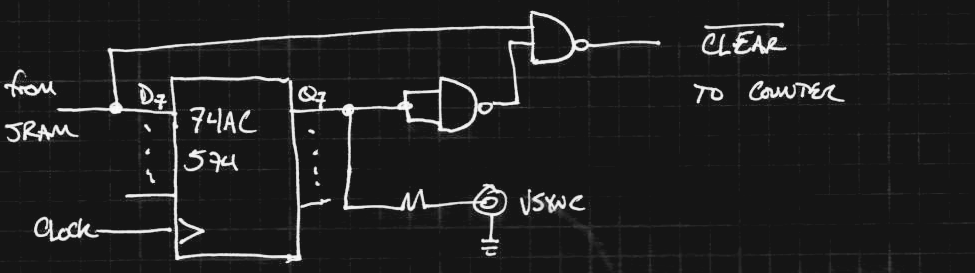
I'm going to document a few places where I'm consciously cutting corners on the design. Here's the first issue - my one-shot circuit for resetting the address counter on the rising edge of Vsync is a poor design. I think it will work, but it's not done "the right way," and that bugs me. I think this is how it should be done:

In this design, the previous state of the vsync line is always stored in the flip-flop (the '574 and the '74 form a 2-stage shift register). The rising edge of the vsync line is detected with the NAND gate (74AC00, but unlabeled in the diagram). This would mean an extra gate package on the board for the NAND, which I'm reluctant to do (simplify!). Of course, if I have to, I can always switch over to this design.
It might be possible to simplify this even more by using input to the 74AC574 and the output to create the reset signal - this design is back to one package (a 74AC00 quad NAND).
 The problem with this design is that the SRAM drivers are already looking like they might be a problem (more details in a future log - they're TTL-level outputs, and not very strong ones, either). Once I get the driver issues sorted out (either with a 74ACT574 with TTL thresholds, or a Thevenin resistive termination/pullup combination on the 74AC574 inputs), I can re-evaluate if this design makes sense. It does only use one gate package - in fact, two gates are left over.
Next Up
Gamma correction: The Right Way, The Wrong Way, and what I might end up doing
Discussions
Become a Hackaday.io Member
Create an account to leave a comment. Already have an account? Log In.