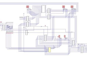
Close
0%
0%

Zinnia (MCPU5)

8 Bit CPU implemented in 100x100µm² IC area for TinyTapeout

timTim
Similar projects worth following

An 8 bit RISC CPU for TinyTapeout. Tinytapeout combines 500 designs on a single IC to be taped out with the Open MPW-7. This offers the opportunity to actually get a design made on a real IC, but also comes with some constraints:

  • Maximum allowed area is 100 x 100 µm² (=0.01 mm²) in Skywater 130nm CMOS technology. The actual number of useable gates depends on cell size and routing limitations.
  • Only eight digital inputs and eight digital outputs are allowed.
  • I/O will be provided via the scanchain (a long shift register) and is hence rather slow.

Designing a CPU around these constraints offers a nice challenge. Challenge accepted!

  • Testing of the actual ASIC

    Tim02/21/2024 at 21:34 0 comments

    I finally received the TinyTapeout board with the Zinnia+ MCU design!


    I decided to use an RP2040 the exercise the I/O of the design. Since the code memory is external to the MCU, it needs to be emulated by a program on the RP2040.

    Here is the output of the prime number generation program:
    ExampleMore documentation and code here: https://github.com/cpldcpu/tt02-mcpu5plus/tree/main/validation

  • Improved Instruction Set Architecture: Zinnia+

    Tim09/07/2022 at 19:56 0 comments

    Post-Tapeout-Regret version: When I implemented the primes example code I noticed some shortcomings of the instructions set architecture that could be easily fixed. The updated version is here on Github, but unfortunatly did not make it on the chip.

    Changes

    Three changes have been introduced:

    1. Allowing the NEG instruction to upgrade the carry. This allows for an easy test for accu=0 or overflow during INC/DEC macros.

    2. Modifying the BCC instruction to read part of the branch target address from the accu, if the iflag is set. This allows for much easier implementation of 8 bit branch target addresses.

    3. Removing JMPA as it was deemed unnecessary with the modification above.

    The resulting instruction set design reduces code size, improves execution speed and even reduces the number of macrocells in the design. A clear win-win.

    Updated Instruction set

    Changes highlighted in red grafik

    Macros using updated instruction set

    grafik

    Benchmark of normal vs. plus version

    grafik

  • Testbench and Assembler

    Tim09/07/2022 at 16:34 0 comments

    You can find the cleaned up designfiles including testbench and assembler on Github.

    I ported two program examples from my other processor designs: Fibonacci number calculation and a prime number search algorithm.

    Fibonacci examples seem to be quite commonplace for minimal processor implementations. However, Fibonacci can be implemented on a machine without any decision making (branching). So, proving that an architecture is able to execute Fibonacci is possibly not a proof of Turing completeness. This is why I prefer the prime number search.

    The Fibonacci implementation is straightforward and shown below:

    .=0
    init:
        LDI  0
        STA  R0  ; a = 0
        LDI  1
        STA  R1  ; b = 1
    loop:
        LDA  R1
        STA  R2  ; temp = b
        
        ADD  R0
        STA  R1  ; b' = a + b
    
        LDA  R2
        STA  R0  ; a = b
    
        OUT      ; display b
    
        BCC loop
    idle:
        BCC idle
    

    The testbench will show the output of the executed programs directly in the shell. In addition, a VCD file with waveforms is generated, which can be viewed with GTKWAVE or the WaveTrace plugin in VSCode.

    grafik

    The number in brackets shows the number of executed program cycles, the output shows the content of the accumulator when the "OUT" instruction in the machine code is executed.

    grafikPrime number sieve:

    ;    divisor=2;    
    ;    while (divisor<number)
    ;    {
    ;        test=-number;
    ;        while (test<0) test+=divisor;
    ;        if (test==0) return 0;
    ;        divisor+=1;
    ;    }
    ;    return 1;
    
    
    number     = R0
    divisor    = R1
    allone     = R7
    
    .=0
    start:
        LDI -1
        STA allone
    
        LDI 2
        STA number
    
        OUT                 ; first prime is 2
    
    outerloop:
        LDI 2
        STA divisor            ;divisor = 2
    
        LDI 1
        ADD number
        STA number
    loop:
        LDA number          ; test=-number;
        NEG
    innerloop:
        ADD    divisor            ; while (test<0) test+=divisor;
        BCCL innerloop
    
        ADD    allone           ; if (test==0) return 0;
        BCCL outerloop       ; No prime
    
        LDI 1               ; divisor+=1;
        ADD    divisor
        STA    divisor
    
        NEG                 ; while (divisor<number)
        ADD number
        BCCL loop
    
    prime:
        LDA number          ; Display prime number
        OUT
    
        JMP outerloop


  • Design Description

    Tim09/06/2022 at 20:32 0 comments

    Top level

    The strict limitations on I/O do not allow implementing a normal interface with bidirectional data bus and separate address bus. One way of addressing this would be to reduce the data width of the CPU to 4 bit, but this was deemed to limiting. Another option, implementing a serial interface, appeared too slow and too complex.

    Instead the I/Os were allocated as shown below.

    The CPU is based on the Harvard Architecture with separate data and program memories. The data memory is completely internal to the CPU. The program memory is external and is accessed through the I/O. All data has to be loaded as constants through machine code instructions.

    Two of the input pins are used for clock and reset, the remaining ones are reserved for instructions and are six bit in length. The output is multiplexed between the program counter (when clk is '1') and the content of the main register, the Accumulator. Accessing the Accumulator allows reading the program output.

    Programmers Model

    Besides simplifying the external interface, the Harvard Architecture implementation also removes the requirement to interleave code and data access on the bus. Every instruction can be executed in a single clock cycle. Due to this, no state machine for micro-sequencing is required and instructions can be decoded directly from the inst[5:0] input.

    All data operations are performed on the accumulator. In addition, there are eight data registers. The data registers are implemented as a single port memory based on latches, which significantly reduced are usage compared to a two port implementation. The Accu is complemented by a single carry flag, which can be used for conditional branches.

    Handling of constants is supported by the integer flag („I-Flag“), which enables loading an eight bit constant with two consecutive 6 bit opcodes.

    Instruction Set Architecture

    The list of instructions and their encoding is shown below. One challenge in the instruction set design was to encode the target address for branches. The limited opcode size only allows for a four bit immediate to be encoded as a maximum. Initially, I considered introducing an additional segment register for long jumps, but ultimately decided to introduce relative addressing for conditional branches and a long jmp instruction that is fed from the accumulator.

    Having both NOT and NEG may seems excessive, but the implementation was cheap on resources and some instruction sequences could be simplified.

    No boolean logic instructions (AND/OR/NOT/NOR/XOR) are supported since they were not needed in any of my typical test programs.

    grafik

    The table below shows common instruction sequences that can be realized with macros.

    grafik


View all 4 project logs

Enjoy this project?

Share

Discussions

Yann Guidon / YGDES wrote 09/12/2022 at 18:31 point

Damnit you did IT again ! :-D

  Are you sure? yes | no

Tim wrote 09/13/2022 at 19:15 point

Seems I only like to design CPUs when there are some challenges to meet :)

  Are you sure? yes | no

zpekic wrote 09/07/2022 at 01:27 point

Super cool! I looked at the verilog description of the CPU, and seems to me that was very much human written and not generate by the pretty basic visual tool. I assume you used the browser tool to generate the skeleton project on github, with magic ID and then swapped out with own verilog source file there ( https://github.com/cpldcpu/tinytapeout_mcpu5/blob/main/src/user_module_341528610027340372.v ) - if so, that is much more convenient way to integrate into existing tool chain(s).

  Are you sure? yes | no

Tim wrote 09/07/2022 at 06:29 point

Yes, I developed the CPU in verilog. It's already too complex for the web tool, imo.
I will add a cleaned up source and testbench soon.

I also submitted an entry using the webtool, but it is much simpler:


https://hackaday.io/project/183938-circuit-golf-electronic-dice-edition/log/210501-007-tinydice-dice-on-an-asic

  Are you sure? yes | no

zpekic wrote 09/10/2022 at 13:32 point

Yes, I was looking at the code and seems this little device is probably able to replace something to the level of complexity of a CPDL, if not more. The 8 input and 8 output limitation could be overcome with a multiplexing scheme. For example inputs:

- clkin, reset, din3...din0 (external mux selected by s1..s0 feeds in here), 1 free pin for use

Outputs:

- s1..s0 - select outputs (internal clock of the device is clkin/4, and this comes from simple counter 0..3)

- dout3...dout0 (output from internal 16 to 4 mux)

- r/notw - memory read/write signal

- as - address strobe (if device is to output memory addresses)

This way a true 8-bit or even 16-bit (doesn't make sense, I know :-)) device could be wrapped into this pin limitation.

  Are you sure? yes | no

Tim wrote 09/13/2022 at 19:17 point

Yeah, I thought about a multiplexing scheme for a while. However, the I/O in tinytapeout is already quite slow, so adding another layer of multiplexing would have turned this into a very slow device. The current design avoids the need of multiplexing, except on the output.

  Are you sure? yes | no

Ken Yap wrote 09/06/2022 at 21:41 point

TinyTapeout link 404'ed.

  Are you sure? yes | no

Tim wrote 09/06/2022 at 21:44 point

thanks, fixed!

  Are you sure? yes | no

Similar Projects

Does this project spark your interest?

Become a member to follow this project and never miss any updates