 noughtnaut
# Main system board (log resumed from 2022-09-08)
(Yes, this keeps getting pushed further into the future. Soon I will have nothing else left to work with though, and eventually will "have" to get this one done.)
This board holds 18 lighted keys and 6 dial knobs. Shown here without the VFD daughter board.


What I initially thought of as the "VFD section" is really the main board, as it includes the CPU, firmware, communication, sockets for the trackball and jog wheel, and power input. There's also an intriguing little 4-gang piano on the underside; I wonder what it does?
There are so many ICs on this board, I'm going to label them:
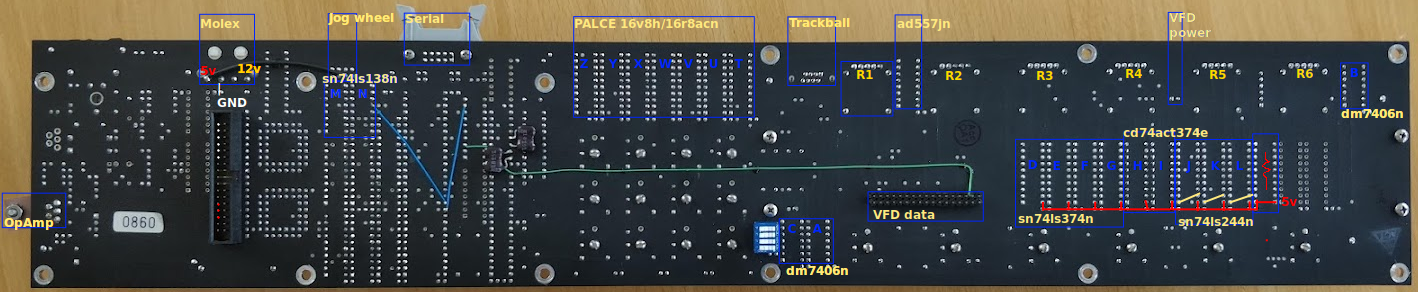
## Power
Diving into the traces of the Molex power socket, it's clear (and unsurprising) that all of the logic runs on 5V. The incandescent bulbs in the 18 key switches are rated for a higher voltage and glow rather dimly if supplied with a measly 5V. Although the bulbs are rated for 14V I am still unsure what this "higher power" voltage is meant to be. I'm going with 12V until I find out otherwise.
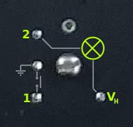
Pin 4 of the Molex connector is wired to 3 places: pin 5 ("+V(s)") of the op-amp jutting out over the edge of the board in the top-left side; to the corresponding solder pad of an empty space that might be intended for another op-amp; and to a power choke (RL1283, labelled "L2", the other side of which eludes my tracing attempts).
The L165 power op-amp is connected thusly:
| Pin | Datasheet | Actual connection |
|---|---|---|
| 5 | +V(s) | Pin 4 (yellow): 12V ?? |
| 4 | Output | GND (wtf really??) |
| 3 | -V(s) | Pin 2 (black): GND |
| 2 | Inverting input | ?? (not yet traced) |
| 1 | Non-inverting input | ?? (not yet traced) |
I don't understand the L165 datasheet well enough to understand what the output on pin 4 is supposed to be. Should it be half-way between the voltages on pins 5 and 3 (so half the voltage on pin 5)?? Are pins 3 and 4 supposed to be tied together, and connect to ground (or is this component busted, or is this just he powered-off state)?? And are pins 1 and 2 important on this board??
Curiously, the final Molex signal (pin 3, white cable) seems to be connected to pin 3 (" -V(s)") of the omitted op-amp; and to another power choke (RL1283 again, labelled "L3"). It must be used for something, but what?? I'm assuming it's just a ground connection.
## Brains
As mentioned, there's a Zilog Z80 in there, alongside an AMD AM85C30 serial controller (these are the two square chips above the Molex socket on the left side of the board), and a bit to the right of them there's a 20MHz crystal. The large brown chip above the serial socket is an AMD AM27C256. Under the 12-button cluster, there's a flock of PALCE16V8H chips.
Close to the serial controller, there's a small (soldered-in) daughter board marked SHUTTLE ENCODER BD which may prove useful for, uh, decoding the jog wheel. That's for later, though.
To the centre-right (which would normally be underneath the VFD daughter board) are four SN74LS374N edge-triggered flip-flops, two (equivalent?) CD74ACT374E flip-flops, and three TI SN74LS244N line drivers. There are two DM7406N logic inverters between the 12-key cluster and the leftmost above-the-VFD key, plus (curiously) a third all the way down in the right-hand corner. Between the two leftmost dial knobs sits a single AD557 8-bit DAC.
### Firmware
For sure, the large brown AMD AM27C256, being a 256kb EPROM, must be the control panel's main firmware.
I am somewhat unsure, though, what the PAL chips represent; according to their datasheets, they are programmable but, as far as I understand, only once (as these do not have windows for UV blanking).
## Switches
I've had no luck finding datasheets for the LKS-2-A 9406 lighted buttons. It's not really important; they're just switches with incandescent bulbs in them, but they are oddly tall and have a sort of military or soviet look to them.

These keys are not wired into the ribbon cable. A pity; that could have provided a nice single source for all button states.
### Sensing
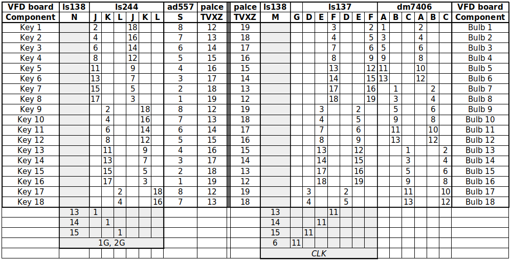
The switched pins (pin 1) of all the keys are pulled high via a resistor ladder (right of "L"); closing the switch pulls their signal low. This output is fed into the SN74LS244 inverters ("J", "K", and ¼ of "L"), whose output enable pins are controlled by one of the multiplexers ("N") over near the jog wheel interface socket. The inverted output then goes to PAL chip ("T") and to the latching DAC ("S").
Meaning, whenever a key is pressed and the corresponding output enable pin is pulled low, the PAL chip gets a high signal on a partucular pin. Keys 1-8 correspond to pins 12-19 on "T" when pin 13 on "M" is high; keys 9-16 correspond to pins 12-19 on "T" when pin 14 on "M" is high; and keys 17 and 18 correspond to pins 12 and 13 on "T" when pin 15 on "M" is high.
What the output of the DAC is used for I've not yet investigated. Given that it's a latching DAC (and that the keys are sensed through multiplexed scanning), it's likely that the DAC serves to store which combination of the 18 keys are active (which will then be used for lighting them, as well as knowing which mode-specific VFD output to provide, and what control inputs are to be interpreted as).
Right now, I'm thinking that this is where I might "cut traces", so that the input/output components talk to my microcontroller instead of the PAL chips (and the rest of the CPU components). In reality, all the relevant chips (the PAL chips "T"-"Z" and the multiplexers "M" and "N") are socketed, so I can simply lift them out and re-use the sockets for prototype wiring. Brilliant. Thanks a lot, Accom!
// TODO Hook up the multiplexer ("N") and the PAL ("T") to my microcontroller and include them in the keyboard scan to read the state of these 18 lighted keys.
### Lighting
The switches contain AML7382 bulbs rated 14V 80mA; apparently, they're typically used in aircraft instruments (so illuminating all bulbs would draw just shy of 1.5 amps).
Lighting the bulbs seem to be controlled by the three DM7406N logic inverters ("A", "B", and "C"), which supply one output for each bulb (pin 2); the other pin of all bulbs connect to the outupt pin of the L165 power op-amp. The 6 inputs of each 7406 come from the 8 outputs of the SN74SL374N latching flip-flops ("D", "E", and "F"), thus utilising 2¼ of the 4 chips. Their inputs are wired in parallel (all pin 3 inputs together, all pin 4 inputs together, etc.), so this puts them in a matrix configuration if their CLK pins are individually addressed -- which indeed they are, from "M" pins 13-15.
Or, seen in the direction of information flow, the PAL chips send data to the AD557 DAC ("S") as well as the three SN74SL374N latching flip-flops ("D", "E", "F") whose outputs are sent through DM7406N inverters ("A", "B", "C") to the light bulbs.
// TODO Hook up the multiplexer ("M") to my microcontroller and see if we can command keys to light up.
### Summary
So far, I have cleared up usage of 6¼ of the 9 chips underneath the VFD, all of the other chips on that side of the board (except what the DAC is used for), and one half of one of the (at least) 7 PAL chips.
It seems that the PAL chips can be used as outputs as well as inputs; I'll have to investigate timing to see just how. But clearly, the same PAL chip pins are used both to read key presses, and to toggle lighting. This might just be clever enough so that pressing a key "automatically" also toggles lighting??
All in all, here is a wiring table of the 18 lighted keys on this board:
## Dial knobs
As for the dial knobs, they're HRPG-ASCA #19R 9323 rotary encoders which provide 120 pulses per revolution. The datasheet recommends combining each with a "HCTL-2016/2020 QUADRATURE DECODER/COUNTER", but here they are routed to the two ACT374E flip-flops ("H", "I") whose outputs are wired into the PAL chips.
// TODO I've yet to look into sensing these dial knobs.
# Current thougths
I would rather not comment on the amount of time finding this out has taken me. Ugh, I am all too aware of my poor understanding of electronics (I pretty much just follow traces and read datasheets) ... but I bet that even so I can make this work as envisioned.
Discussions
Become a Hackaday.io Member
Create an account to leave a comment. Already have an account? Log In.