 Christoph
Table of contents:
- First things first - you're not a factory
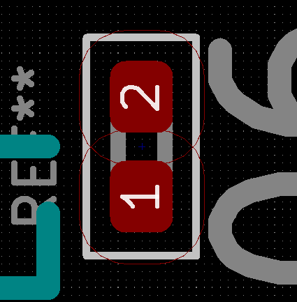
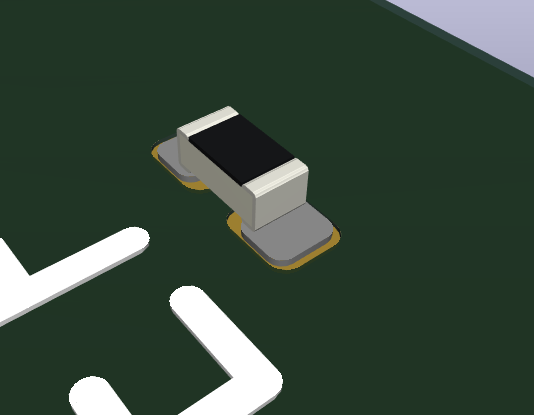
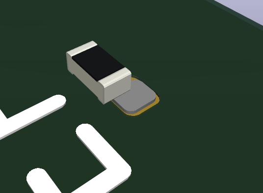
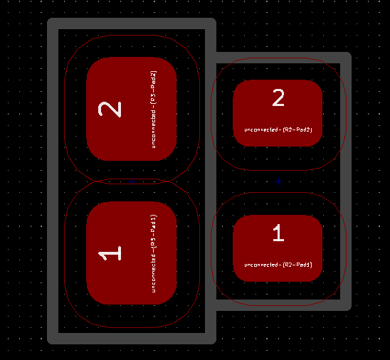
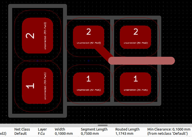
- Placement Accuracy
- Layout: Courtyards, vias in pads, and double-sided assembly
- Combining high temp and low temp solder on the same board
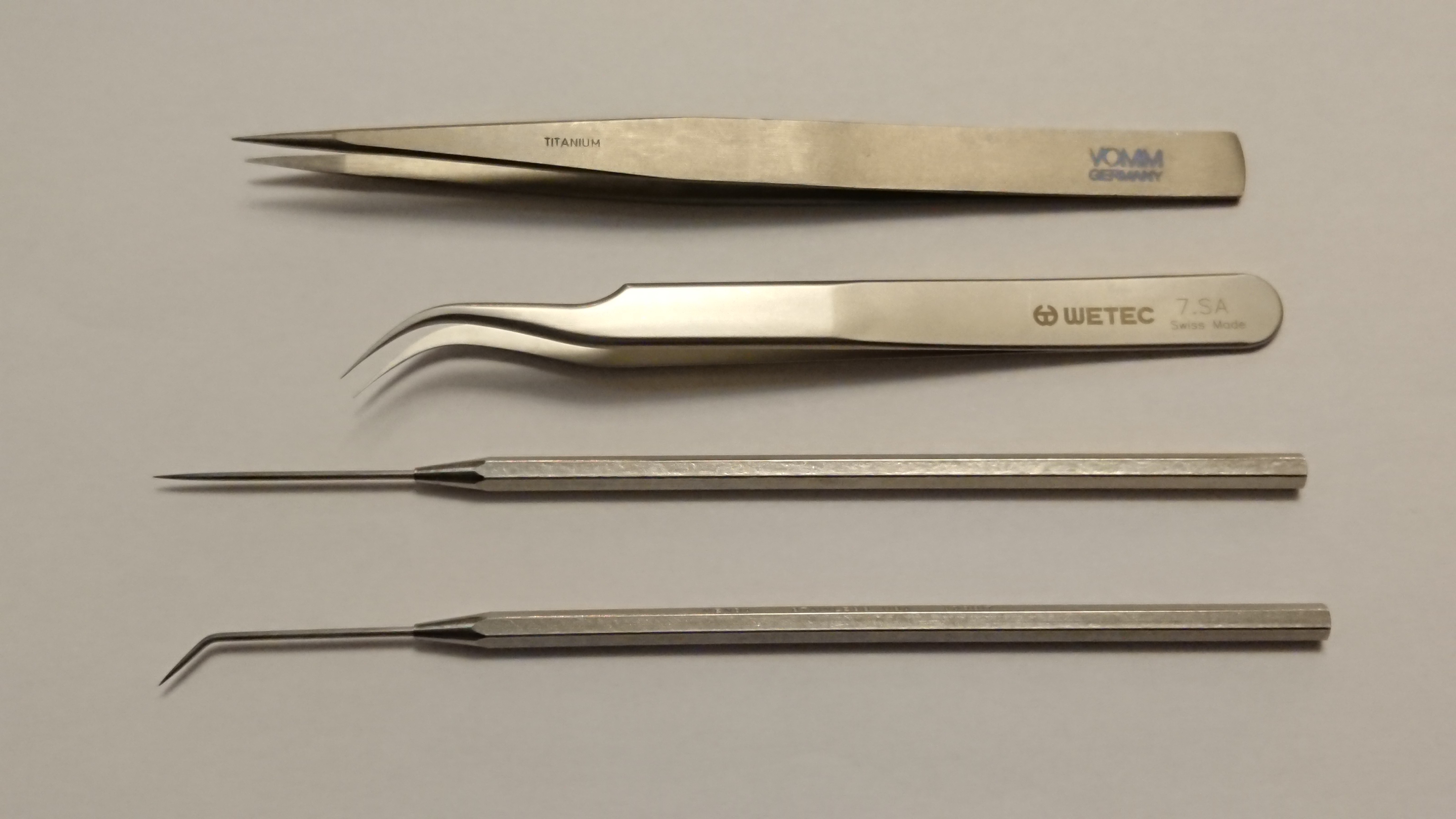
- The paintbrush technique for low temp solder (this might be the most "exciting" part yet)
I'll add more and rearrange them when I have more, of course. Things that will definitely come:
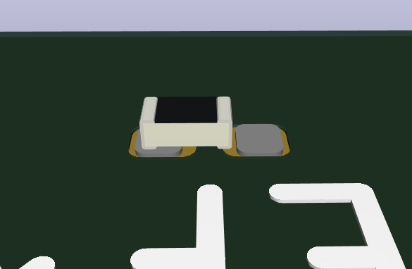
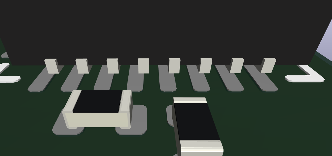
- Really Nasty packages
- Assembly strategy


 deʃhipu
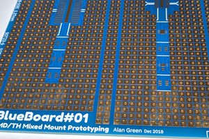
 Alan Green
 Jean Simonet
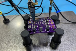
 tonyo
tonyo
Nice, I might want to do something small anytime and your tips are really helpful!